Electroluminescence device and manufacturing method thereof

An electroluminescence device and photoresist technology, which is applied to circuits, electrical components, electrical solid devices and other directions, can solve the problems of difficulty in etching the connecting electrode 14 and take a long time, so as to reduce the difficulty of etching, improve the yield, The effect of shortening the film formation time

Active Publication Date: 2013-12-25
BOE TECH GRP CO LTD
View PDF5 Cites 13 Cited by
  • Summary
  • Abstract
  • Description
  • Claims
  • Application Information

AI Technical Summary

Problems solved by technology

[0004] In order to fully contact the connecting electrode 14 and the second electrode 26 behind the box, and improve the reliability of the electrical connection between the thin film transistor 12 and the second electrode 26, the connecting electrode 14 is usually prepared relatively thick (generally 2-3 microns), but this It will cause firstly that the process of forming a thin film during preparation takes a long time, and secondly, it will be difficult to etch when etching the thin film to form the connecting electrode 14

Method used


Image

  • Electroluminescence device and manufacturing method thereof
  • Electroluminescence device and manufacturing method thereof
  • Electroluminescence device and manufacturing method thereof

Examples


Embodiment 1

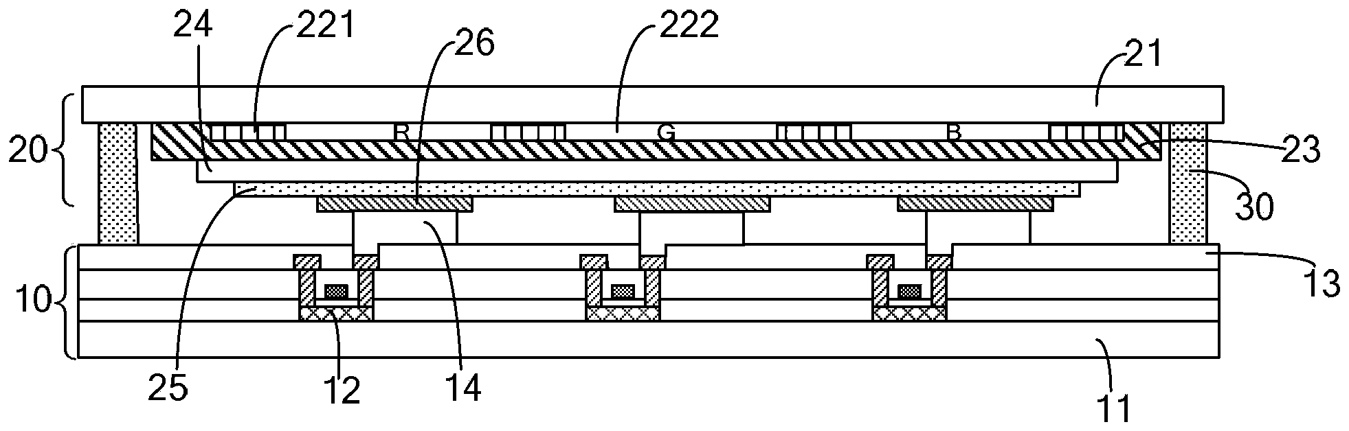
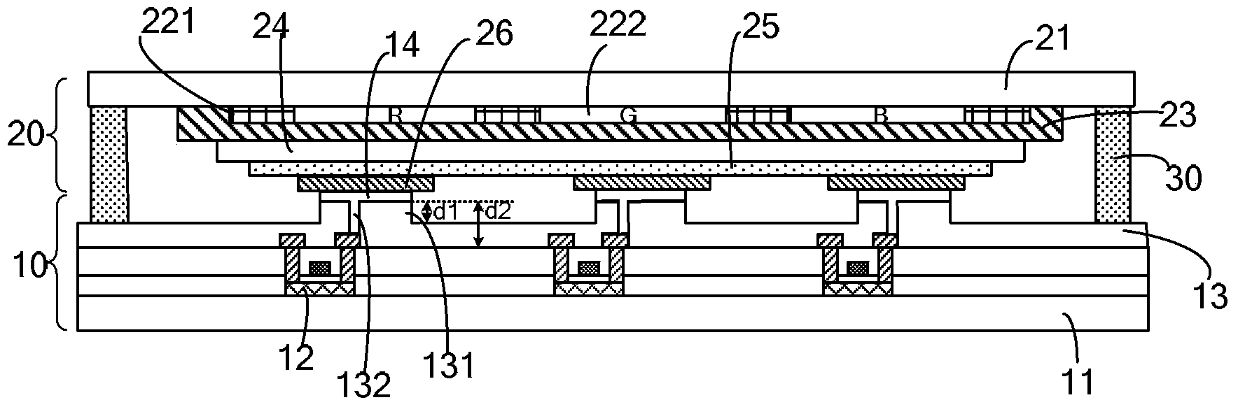
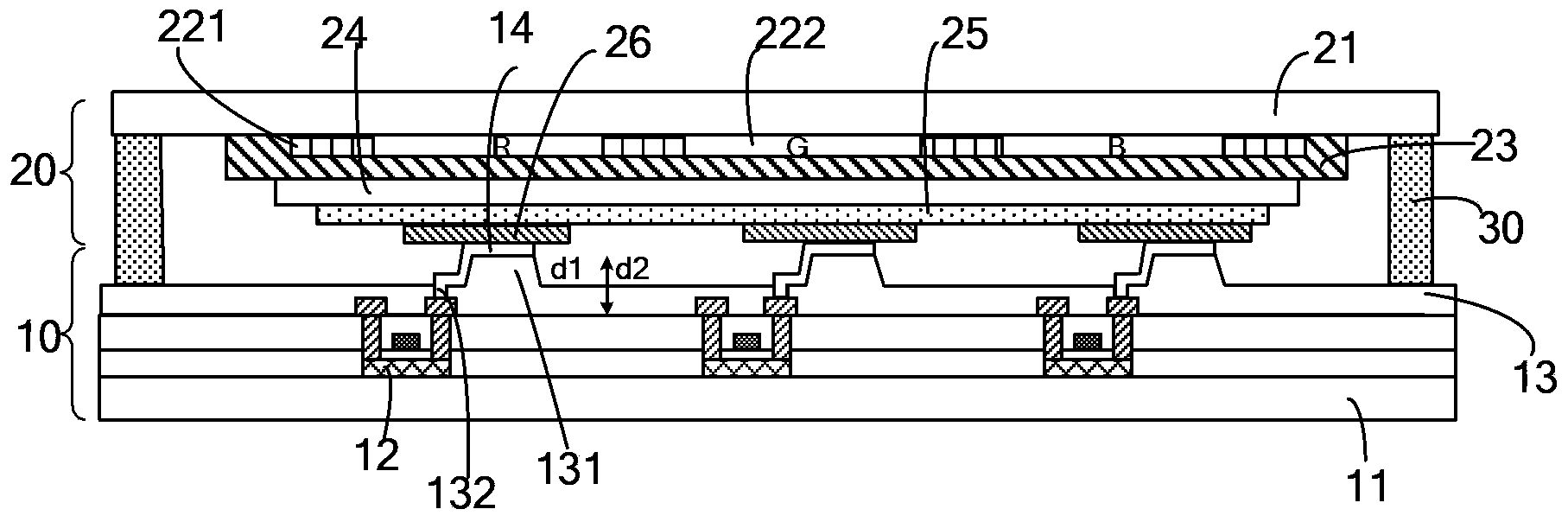
[0061] An embodiment of the present invention provides an electroluminescence device, as shown in FIG. 2(a) and FIG. 2(b), the device includes: an array substrate 10; the array substrate 10 includes: a substrate 11, and the The thin film transistor 12, the protective layer 13 covering the thin film transistor 12, and the connection electrode 14 arranged on the protective layer 13; the protective layer 13 below the connection electrode 14 protrudes to the side away from the substrate 11, forming a boss 131 ; the protective layer 13 is provided with a protective layer via hole 132 at a position corresponding to the drain of the thin film transistor 12 , and the connection electrode 14 is connected to the drain of the thin film transistor 12 through the protective layer via hole 132 .

[0062] A TFT circuit (driver circuit) is provided on the array substrate 10 for driving and compensating the OELD. There are many ways to implement the driving circuit, but the driving circuit at ...

Embodiment 2

[0073] The embodiment of the present invention also provides a method for manufacturing an electroluminescence device, the preparation method includes: a color filter substrate manufacturing process, an array substrate manufacturing process, a color filter substrate and an array substrate manufacturing process, wherein, such as image 3 As shown, the array substrate manufacturing process includes:

[0074] Step 101, forming a thin film transistor 12 on the substrate 11;

[0075] Step 102: Form a protective layer 13 on the substrate on which the thin film transistor 12 is formed, and form a boss 131 at a predetermined position where the connection electrode is subsequently formed through a patterning process, and form a protective layer via hole 132 at a position corresponding to the drain of the thin film transistor 12 ;

[0076] Step 103 , forming a connection electrode 14 on the protection layer 13 , and connecting the connection electrode 14 to the drain of the thin film t...


PUM


Abstract

An embodiment of the invention discloses an electroluminescence device and a manufacturing method thereof, and relates to the display field. The reliability of electric connection of a thin film transistor and a second electrode is ensured, and in the meanwhile, film forming time can be shortened, the etching difficulty can be reduced and accordingly the production efficiency can be improved in the connecting electrode manufacturing process. The electroluminescence device comprises an array substrate, wherein the array substrate comprises a substrate body, thin film transistors sequentially arranged on the substrate body, protective layers covering the thin film transistors and connecting electrodes arranged on the protective layers. The protective layers under the connecting electrodes protrude towards one side away from the substrate body to form bosses. Protective layer through holes are formed in the positions, corresponding to drain electrodes of the thin film transistors, of the protective layers, and the connecting electrodes are connected with the drain electrodes of the thin film transistors through the protective layer through holes.

Description

technical field [0001] The invention relates to the display field, in particular to an electroluminescent device and a preparation method thereof. Background technique [0002] Organic Light Emitting Diode (OLED), also known as Organic Electroluminescence Display (OELD), has self-illumination, no backlight, high contrast, thin thickness, wide viewing angle, fast response, With its excellent characteristics such as wide operating temperature range, simple structure and manufacturing process, it has been widely used in mobile communication terminals, personal digital assistants (PDAs), and handheld computers recently. [0003] Such as figure 1 As shown, an existing active matrix OLED display device includes: a color filter substrate 20 and an array substrate 10, wherein the array substrate 10 includes: a substrate 11, an array of thin film transistors 12 sequentially arranged on the substrate 11, and a protective layer 13 and a connection electrode 14, the connection electro...

Claims


Application Information

Patent Timeline
Patent Type & Authority Applications(China)
IPC IPC(8): H01L27/32H01L51/56
CPCH10K59/38H10K59/123H10K59/1275H10K59/124H10K71/50H10K59/1201H10K2102/351H10K2102/00
Inventor 程鸿飞张玉欣
Owner BOE TECH GRP CO LTD
Why Eureka
Try Eureka