Cell structure of super junction semiconductor device and technology realizing method

A super junction and semiconductor technology, applied in semiconductor devices, semiconductor/solid-state device manufacturing, electrical components, etc., can solve problems such as device damage and increased avalanche tolerance of devices

Inactive Publication Date: 2014-01-01
上海恺创电子有限公司 +1
View PDF9 Cites 3 Cited by
  • Summary
  • Abstract
  • Description
  • Claims
  • Application Information

AI Technical Summary

Problems solved by technology

When the avalanche energy acts on the device, the heat of the device exceeds the limit that the device itself can withstand, and the device is damaged
And as figure 2 As shown, when the device undergoes avalanche breakdown, the temperature of the device continues to rise and the parasitic transistor is turned on, resulting in a significant increase in the avalanche tolerance of the device

Method used


Image

  • Cell structure of super junction semiconductor device and technology realizing method
  • Cell structure of super junction semiconductor device and technology realizing method
  • Cell structure of super junction semiconductor device and technology realizing method

Examples


Embodiment Construction

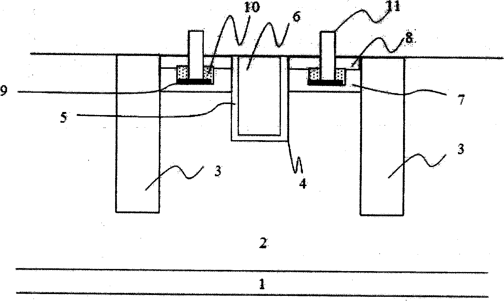
[0019] The invention discloses a cell structure and process realization method of a deep-groove super junction semiconductor device, including a first-type heavily doped region [1] of the substrate of the device; located in the first-type heavily-doped region of the substrate The first type of epitaxial drift region [2] above [1]; the second type of epitaxial column region [3] located above the substrate heavily doped region [1] and on both sides of the epitaxial drift region [2] ]; there is a gate trench [4] between the second type of epitaxial column area [3]; the gate polysilicon [6] is inside the trench; the gate trench [4] is connected to the gate There is a dielectric isolation layer [5] between the extremely polysilicon [6]; a second-type doped well region [7] is formed between the gate trench [4] and the semi-insulating column region [3]; the The source region [8] doped with the first type is formed on the upper part of the well region; the source region [8] and the we...


PUM

PropertyMeasurementUnit
Thicknessaaaaaaaaaa

Abstract

The invention discloses a deep-groove-type cell structure of a super junction semiconductor device and a technology realizing method. The cell structure comprises a first-type heavily doped region, a first-type epitaxial drift region is arranged on the first-type heavily doped region, second-type epitaxial column regions are arranged on the two sides inside the epitaxial drift region, a grid groove is formed between the second-type epitaxial column regions, a grid polysilicon and dielectric isolation layer is arranged inside the groove, a second-type doped well region is formed between the grid groove and a semi-insulation column region, a first-type doped source region is formed on the upper portion of the well region, a second-type epitaxial region is arranged inside the second-type doped well region, and a metal buried layer is arranged under the second-type epitaxial region. The deep-groove-type cell structure can effectively reduce series resistance of the well region of the super junction product, prevent opening of parasitic transistors, and therefore the avalanche breakdown resistance capacity of the device is improved, and the related reliability of the product is improved.

Description

technical field [0001] The invention relates to a super-junction device structure in a semiconductor integrated circuit, in particular to a structural design and process realization method of a deep-groove super-junction semiconductor device. Background technique [0002] Superjunction semiconductor devices are the intrinsic driving force of ever-evolving power-electronic systems. Especially in terms of energy saving, dynamic control, noise reduction and so on. The product is mainly used to control the energy between the energy source and the load, and should have the characteristics of high precision, fast speed and low power consumption. [0003] However, the application of superjunction devices is limited by their avalanche tolerance. like image 3 As shown, when the super junction device is turned off instantaneously (the gate voltage of the product drops to 0 or negative voltage), due to the presence of load current, the inductive load acts as a negative current sourc...

Claims


Application Information

Patent Timeline
IPC IPC(8): H01L21/336H01L29/78H01L29/49
CPCH01L29/0634H01L29/66666H01L29/0856H01L29/41766H01L29/66727H01L29/7813
Inventor 张志群张峰
Owner 上海恺创电子有限公司
Why Eureka
Try Eureka