Method for forming semiconductor packaging structure

A packaging structure and semiconductor technology, which is applied in the direction of semiconductor devices, semiconductor/solid-state device manufacturing, semiconductor/solid-state device components, etc., can solve the problems of poor reliability of packaging structures and prone to failure, so as to improve stability and reliability, The effect of increasing adhesion

Active Publication Date: 2014-01-01
NANTONG FUJITSU MICROELECTRONICS
View PDF2 Cites 5 Cited by
  • Summary
  • Abstract
  • Description
  • Claims
  • Application Information

AI Technical Summary

Problems solved by technology

[0010] However, the reliability of the existing package structure is poor, and it is prone to failure

Method used


Image

  • Method for forming semiconductor packaging structure
  • Method for forming semiconductor packaging structure
  • Method for forming semiconductor packaging structure

Examples


Embodiment Construction

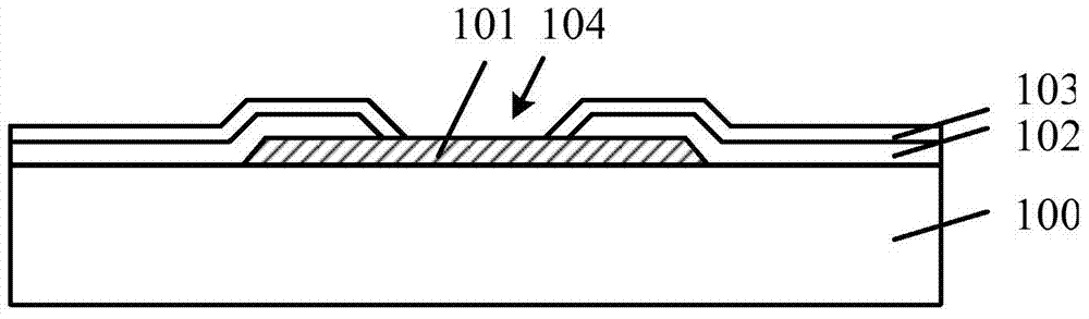
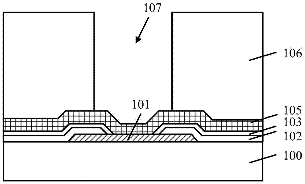
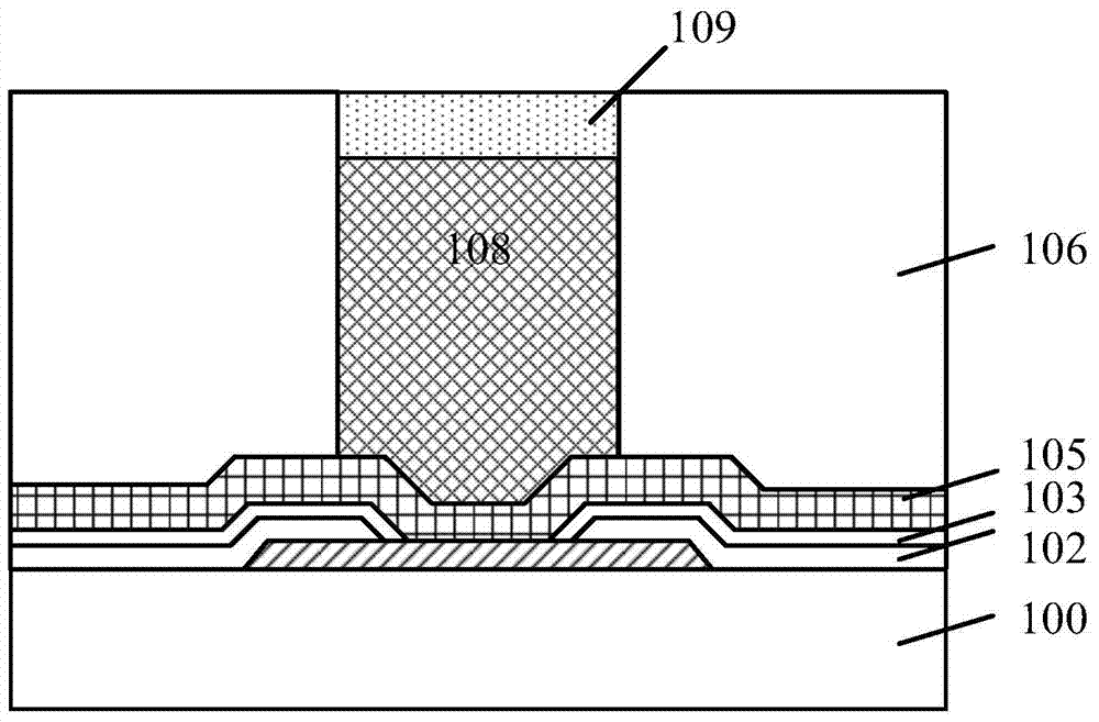
[0027] After research, it is found that the existing maskless wet etching method to remove the under-convex metal layer not covered by the metal pillars is prone to undercut defects. For details, please refer to image 3 and Figure 4 , when the metal post 108 is used as a mask to remove the metal layer 105 under the protrusion on the polymer layer 103 on both sides of the metal post 108 by wet etching, due to the isotropic property of wet etching, the removal of the metal under the protrusion layer 105 , it is easy to over-etch the part of the raised metal layer 105 under the metal pillar 108 , so that the remaining raised metal layer 105 under the metal pillar 108 is inwardly depressed to form an undercut defect 112 . The existence of the undercut defect 112 will make the bottom part of the metal pillar 108 suspended, so that the contact area between the metal pillar 108 and the metal layer 105 under the protrusion is reduced, and the adhesion between the metal pillar 108 an...


PUM


Abstract

A method for forming a semiconductor packaging structure comprises the steps of providing a semiconductor substrate and enabling a welding pad layer to be formed on the semiconductor substrate; forming a passivation layer covering the semiconductor substrate and part of the surface of the welding pad layer and enabling the passivation layer to be provided with a first opening which exposes part of the surface of the welding pad layer; forming concave metal layers on a side wall and the bottom of the first opening and the passivation layer; forming a first mask layer covering the concave metal layers and enabling the first mask layer to be provided with a second opening exposing part of the concave metal layers on the first opening; forming a metal column in the second opening; removing the first mask layer; forming a bottom layer metal layer on a side wall of the bottom of the metal column and part of the surfaces of the concave metal layers; removing second mask layers; and enabling the metal column and the bottom layer metal layer to serve as masks to remove the concave metal layers on two sides of the metal column by etching. According to the method, undercutting defects of the concave metal layers below the metal column are avoided.

Description

technical field [0001] The invention relates to the field of semiconductor packaging, in particular to a method for forming a semiconductor packaging structure. Background technique [0002] Semiconductor packaging refers to the process of processing wafers according to product models and functional requirements to obtain independent chips. Existing semiconductor packages include wire-bonding packages and flip-chip packages. Compared with the wire bonding packaging method, the flip chip packaging method has the advantages of high packaging density, excellent heat dissipation performance, high input / output (I / O) port density and high reliability. [0003] In the earlier flip-chip packaging method, pads are provided on the chip, and the bumps provided on the pads (including input / output pads) are used to weld with the packaging substrate to realize chip packaging. With the development of the semiconductor industry in the direction of miniaturization, the density of chips for...

Claims


Application Information

Patent Timeline
IPC IPC(8): H01L21/60H01L23/485
CPCH01L24/11H01L21/4853H01L2224/02126H01L2224/03001H01L2224/1147H01L2224/11903H01L2224/11906
Inventor 石磊陶玉娟
Owner NANTONG FUJITSU MICROELECTRONICS
Why Eureka
Try Eureka