Light emitting diode with reflector protective layer

A technology of light-emitting diodes and protective layers, applied in electrical components, circuits, semiconductor devices, etc., can solve the problems of silver oxidation, reduction of light-emitting efficiency of light-emitting diodes, reduction of reflection efficiency of reflective layer 4, etc.

Inactive Publication Date: 2014-01-01
HIGH POWER OPTO
View PDF7 Cites 1 Cited by
  • Summary
  • Abstract
  • Description
  • Claims
  • Application Information

AI Technical Summary

Problems solved by technology

[0005] However, after forming the reflective layer 4 under the P-type semiconductor layer 3, the light-emitting diode must continue to form the buffer layer 5, the bonding layer 6, etc. under the reflective layer 4, and it needs to go through multiple semiconductor processes. Therefore, the silver in the reflective layer 4 is easily oxidized due to the subsequent process, which will reduce the reflection efficiency of the reflective layer 4 and reduce the light extraction efficiency of the light emitting diode.

Method used


Image

  • Light emitting diode with reflector protective layer
  • Light emitting diode with reflector protective layer
  • Light emitting diode with reflector protective layer

Examples


Embodiment Construction

[0018] Hereby, the detailed content and technical description of the present invention are further described with examples.

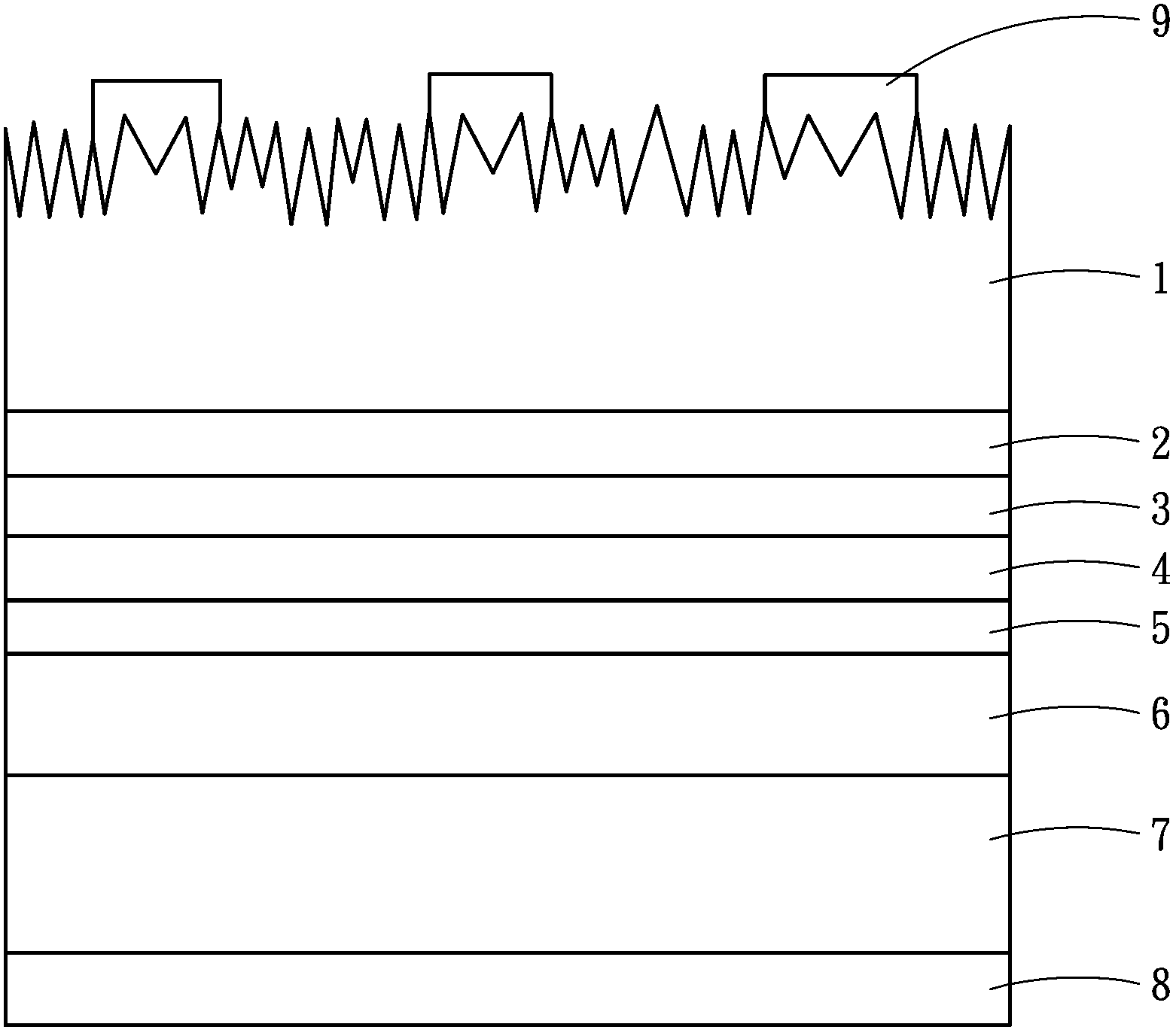
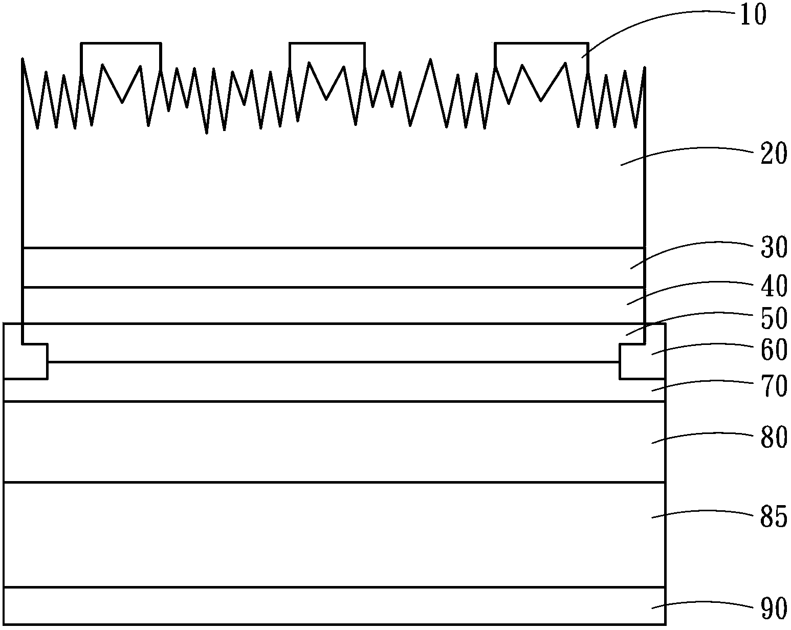
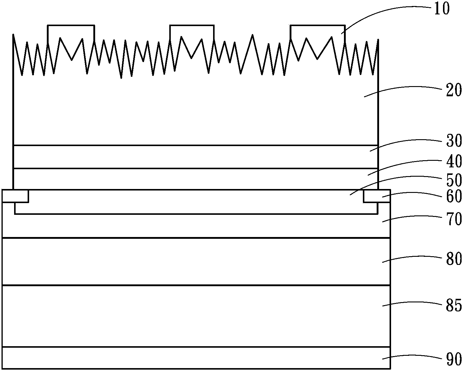
[0019] see again figure 2 and image 3 As shown, the present invention is a light-emitting diode with a mirror protection layer, which includes an N-type electrode 10, an N-type semiconductor layer 20, a light-emitting layer 30, a P-type semiconductor layer 40, a metal reflective layer 50, A protection layer 60 , a buffer layer 70 , a bonding layer 80 , a permanent substrate 85 and a P-type electrode 90 .

[0020] Wherein the N-type electrode 10 is formed on one side of the N-type semiconductor layer 20, the light-emitting layer 30 is formed on the side of the N-type semiconductor layer 20 away from the N-type electrode 10, and the P-type semiconductor layer 40 is formed on the light-emitting layer. The side of the layer 30 away from the N-type semiconductor layer 20 , the sandwich structure formed by the N-type semiconductor layer 20 , the light-emi...


PUM

PropertyMeasurementUnit
thicknessaaaaaaaaaa
thicknessaaaaaaaaaa
thicknessaaaaaaaaaa

Abstract

The invention discloses a light emitting diode with a reflector protective layer. The light emitting diode comprises an N-type electrode, an N-type semiconductor layer, a light emitting layer, a P-type semiconductor layer, a metal reflecting layer, the protective layer, a buffering layer, a combination layer, a permanent substrate and a P-type electrode, wherein the N-type electrode, the N-type semiconductor layer, the light emitting layer, the P-type semiconductor layer, the metal reflecting layer, the protective layer, the buffering layer, the combination layer, the permanent substrate and the P-type electrode are sequentially stacked, the protective layer is made of metallic oxide and forms a hollowed frame pattern, the edge of the metal reflecting layer is covered or supported with the frame pattern, therefore, the metal reflecting layer can be protected through surrounding and shielding of the protective layer and prevented from being oxidized in the follow-up manufacturing process, the deserved reflectivity of the metal reflecting layer can be maintained, and accordingly the light emitting efficiency and the electrical stability of the light emitting diode are improved.

Description

technical field [0001] The invention relates to light emitting diodes, in particular to a structure for increasing light extraction efficiency of the light emitting diodes. Background technique [0002] A light emitting diode (Light Emitting Diode; LED) is mainly composed of multiple epitaxial stacks of semiconductor materials. Taking a blue light emitting diode as an example, it is mainly composed of a gallium nitride-based (GaN-based) epitaxial thin film. [0003] see figure 1 As shown, it is an existing vertical light-emitting diode, which includes an N-type semiconductor layer 1, a light-emitting layer 2 and a P-type semiconductor layer 3 in a sandwich structure, and a Reflective layer 4, a buffer layer 5 (Buffer layer), a bonding layer 6, a silicon substrate 7 and a P-type electrode 8, and the surface of the N-type semiconductor layer 1 can be roughened to increase the light output rate, and provide An N-type electrode 9 is provided, and accordingly, after a voltage i...

Claims


Application Information

Patent Timeline
Patent Type & Authority Applications(China)
IPC IPC(8): H01L33/00
CPCH01L33/44H01L33/46H01L2933/0025
Inventor 颜伟昱周理评陈復邦张智松
Owner HIGH POWER OPTO
Why Eureka
Try Eureka