
Reaction chamber and thin film deposition equipment

A reaction chamber and chamber technology, which are applied in the field of reaction chambers and thin film deposition equipment, can solve the problems of increasing the loss of radiated heat of a heating bulb 13, reducing the processing efficiency of thin film deposition equipment, reducing heating efficiency, etc., so as to improve the eddy current The effect of distribution, processing efficiency improvement, and heating efficiency improvement

Active Publication Date: 2015-12-02
BEIJING NAURA MICROELECTRONICS EQUIP CO LTD
View PDF3 Cites 0 Cited by
  • Summary
  • Abstract
  • Description
  • Claims
  • Application Information

AI Technical Summary

Problems solved by technology

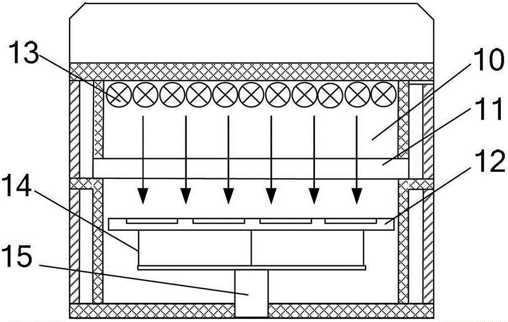
[0007] First, since the heating bulb 13 is arranged in the atmosphere, the heat is easily lost, resulting in a slow rise in the temperature of the processed workpiece such as the substrate, thereby reducing the processing efficiency of the thin film deposition equipment
[0008] Second, the heat of the heating bulb 13 needs to pass through the quartz window 11 to radiate into the lower chamber, and the quartz window 11 will reflect part of the heat to the heating bulb 13, thereby increasing the heat loss of the heating bulb 13 and reducing the heating efficiency. This in turn reduces the processing efficiency of thin film deposition equipment

Method used


Image

  • Reaction chamber and thin film deposition equipment
  • Reaction chamber and thin film deposition equipment
  • Reaction chamber and thin film deposition equipment

Examples


Embodiment Construction

[0036] In order to enable those skilled in the art to better understand the technical solutions of the present invention, the reaction chamber and thin film deposition equipment provided by the present invention will be described in detail below with reference to the accompanying drawings.

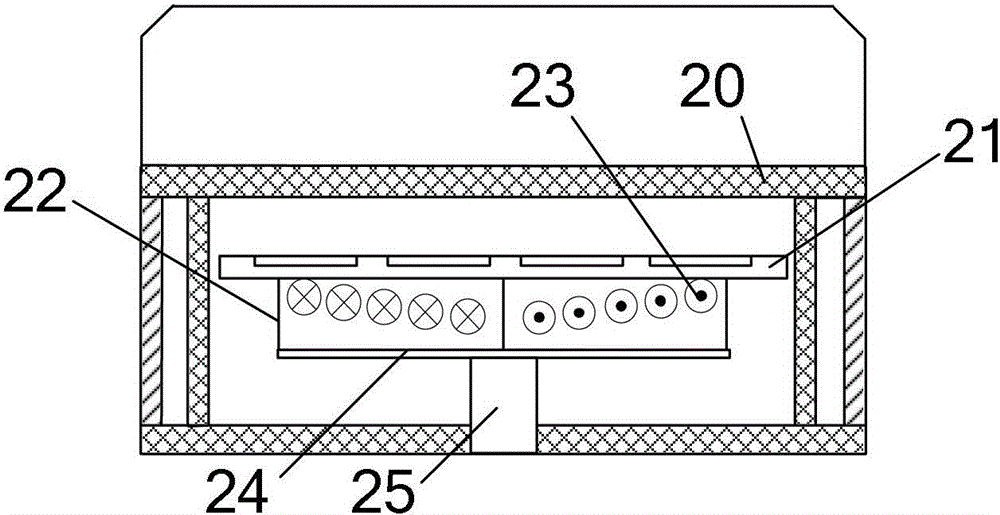
[0037] Figure 2a Schematic diagram of the structure of the reaction chamber provided by the first embodiment of the present invention. see Figure 2a , the reaction chamber includes a chamber body 20, a tray 21, a carrier, an induction coil 23 and an AC power supply (not shown in the figure). Wherein, the carrying part is disposed in the chamber body 20 for carrying the tray 21 . The tray 21 is used to carry the processed workpiece, which is made of magnetically permeable materials such as graphite, silicon carbide or magnetically permeable metal.

[0038] The induction coil 23 is disposed in the chamber body 20 and below the tray 21 , and is connected to an AC power source. When heat...


PUM


Abstract

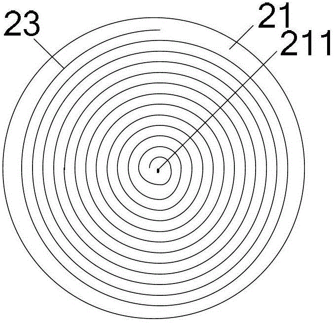
The invention provides a reaction chamber and a thin film deposition device. The reaction chamber includes a chamber body and a tray which is used for bearing a processed workpiece, a bearing component for bearing the tray is arranged in the chamber body, and the tray is characterized by being made of a magnetic-conductivity material; and moreover, an induction coil arranged below the tray is of a funnel shape and comprises a multi-turn coil formed by being wound in a spiral mode, and the axis of the induction coil is coincided with the axis of the tray; the induction coil is connected with an alternating current power supply, eddy current generated in the tray and generated with the help of an alternating magnetic field generated by the induction coil is used for heating the tray, and then the processed workpiece is heated. The reaction chamber has less heat loss, high heating efficiency and uniform heating, and can improve the processing efficiency of the thin film deposition device.

Description

technical field [0001] The invention relates to the technical field of microelectronic processing, in particular to a reaction chamber and thin film deposition equipment. Background technique [0002] Physical vapor deposition (Physical Vapor Deposition, hereinafter referred to as PVD) technology is a commonly used processing technology in the field of microelectronics, for example, it is used to prepare tin-doped indium oxide (IndiumTinOxide, hereinafter referred to as ITO) thin film on a sapphire substrate. When implementing the process, the sapphire substrate needs to be heated to ensure that the ITO film deposited on the sapphire substrate can crystallize normally. [0003] see figure 1 , figure 1 It is a structural schematic diagram of an existing PVD device. , the PVD apparatus includes a reaction chamber 10 and a tray 12 and a robot (not shown in the figure) for transferring the tray 12 . A quartz window 11 is provided inside the reaction chamber 10 , and the reac...

Claims


Application Information

Patent Timeline
Patent Type & Authority Patents(China)
IPC IPC(8): C23C14/22C23C14/08
Inventor 叶华刘菲菲
Owner BEIJING NAURA MICROELECTRONICS EQUIP CO LTD
Learn More