FinFET manufacturing method

A manufacturing method and substrate technology, applied in semiconductor/solid-state device manufacturing, electrical components, circuits, etc., can solve the problems of reducing FinFET device performance, high-k dielectric layer Fermi level pinning, and charge trap effects, etc. Improve the effect of Fermi level pinning, reduce bandgap states or oxygen vacancies, and improve threshold voltage drift

Inactive Publication Date: 2014-01-15
SEMICON MFG INT (SHANGHAI) CORP
View PDF7 Cites 13 Cited by
  • Summary
  • Abstract
  • Description
  • Claims
  • Application Information

AI Technical Summary

Problems solved by technology

[0006] However, in the prior art, the gate dielectric layer formed using a high-k dielectric material (such as Hf) has poor bonding performance with the silicon in the fin-shaped channel region 13, and the bonding performance between the gate dielectric layer and the silicon in the fin-shaped channel region 13 is poor. The bandgap state or oxygen vacancies are induced at the interface, resulting in the Fermi level pinning problem in the high-k dielectric layer, which makes the silicon interface of the fin-shaped channel region 13 uneven, thereby increasing the stacking gap between the high-k dielectric layer and the gate layer. The number of defects in the gate structure 14 makes it suffer from severe charge trapping, resulting in threshold voltage shift and degrading the performance of FinFET devices

Method used


Image

  • FinFET manufacturing method
  • FinFET manufacturing method
  • FinFET manufacturing method

Examples


Embodiment Construction

[0028] The FinFET manufacturing method proposed by the present invention will be further described in detail below with reference to the accompanying drawings and specific embodiments.

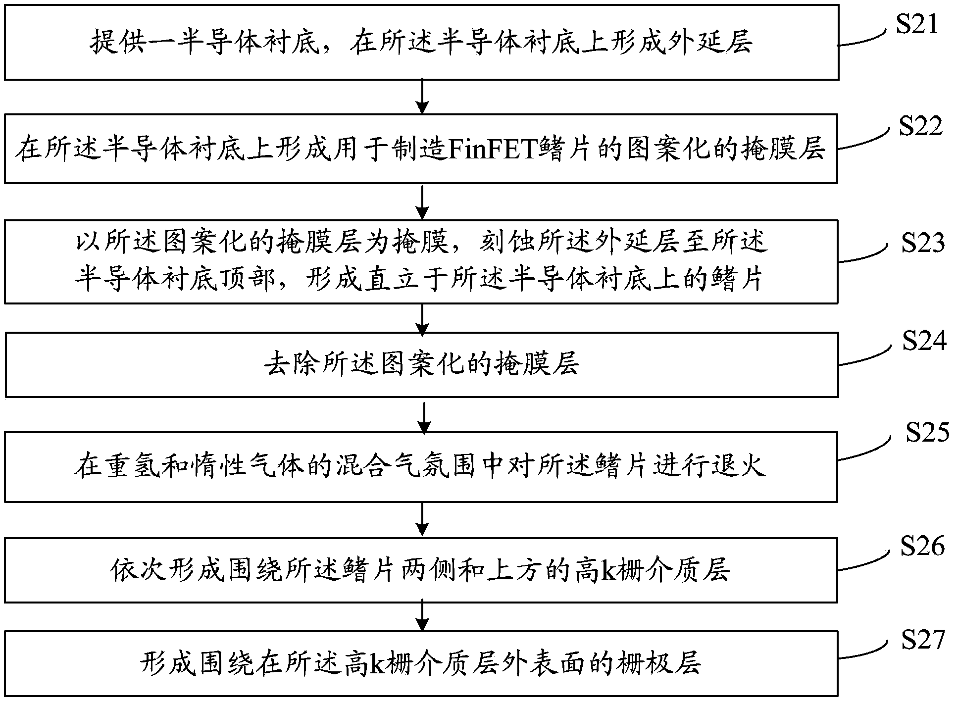
[0029] Such as figure 2 As shown, the present invention provides a kind of FinFET manufacturing method, comprises the following steps:

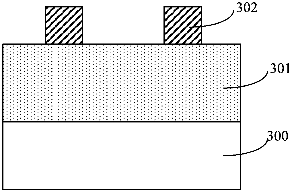
[0030] S21, providing a semiconductor substrate, forming an epitaxial layer on the semiconductor substrate;

[0031] S22, forming a patterned mask layer for manufacturing FinFET fins on the semiconductor substrate;

[0032] S23. Using the patterned mask layer as a mask, etch the epitaxial layer up to the top of the semiconductor substrate to form fins standing on the semiconductor substrate.

[0033] S24, removing the patterned mask layer;

[0034] S25, annealing the fins in a mixture gas atmosphere of deuterium and inert gas

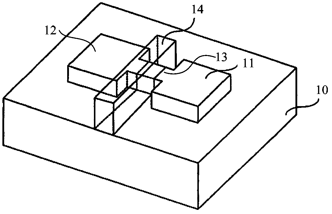
[0035] S26, forming a high-k gate dielectric layer surrounding both sides and above the fin;

[0036] S27, forming a gate layer...


PUM

PropertyMeasurementUnit
thicknessaaaaaaaaaa

Abstract

The invention provides a FinFET manufacturing method. Before or after a step of forming a high-k gate dielectric layer surrounding the two sides and the upper side of a fin, the fin is annealed in a mixed atmosphere of heavy hydrogen and inert gas, dangling bonds of silicon in the fin are eliminated, induced band gap state or oxygen vacancy at a fin interface are reduced, the problem of Fermi energy level pinning in the high-k dielectric layer is improved, and the fin interface is smoothed, thereby reducing the number of defects in the high-k dielectric layer, suppressing the charge trap effect, improving the threshold voltage drift and improving the performance of FinFET devices.

Description

technical field [0001] The invention relates to the field of semiconductor manufacturing, in particular to a FinFET manufacturing method. Background technique [0002] MOSFET (Metal Oxide Semiconductor Field Effect Transistor) is the main component of most semiconductor devices. When the channel length is less than 100nm, in the traditional MOSFET, due to the semiconductor material of the semiconductor substrate surrounding the active region, the source and drain regions Interaction, the distance between the drain and the source is also shortened, resulting in a short channel effect, so that the control ability of the gate to the channel becomes worse, and it becomes more and more difficult for the gate voltage to pinch off the channel The larger the value, the easier it is for the subthrehhold leakage phenomenon to occur. [0003] Fin field effect transistor (Fin Field effect transistor, FinFET) is a new metal oxide semiconductor field effect transistor, its structure is u...

Claims


Application Information

Patent Timeline
Patent Type & Authority Applications(China)
IPC IPC(8): H01L21/324H01L21/336
CPCH01L29/66795H01L21/28185
Inventor 赵猛
Owner SEMICON MFG INT (SHANGHAI) CORP
Why Eureka
Try Eureka