GaN-base light-emitting diode chip growing method

A technology of light-emitting diodes and growth methods, which is applied in the field of growth of GaN-based light-emitting diode chips, can solve problems such as low luminous efficiency, low hole injection efficiency of light-emitting diode chips, and limited effects, so as to improve luminous efficiency and injection and crystal quality, the effect of increasing efficiency

Active Publication Date: 2014-01-15
HC SEMITEK CORP
View PDF4 Cites 19 Cited by
  • Summary
  • Abstract
  • Description
  • Claims
  • Application Information

AI Technical Summary

Problems solved by technology

[0005] In prior art at N 2 and H 2 Growing the p-type layer in a mixed atmosphere has a limited effect on improving the quality of the p

Method used


Image

  • GaN-base light-emitting diode chip growing method

Examples


Example Embodiment

[0025] Example

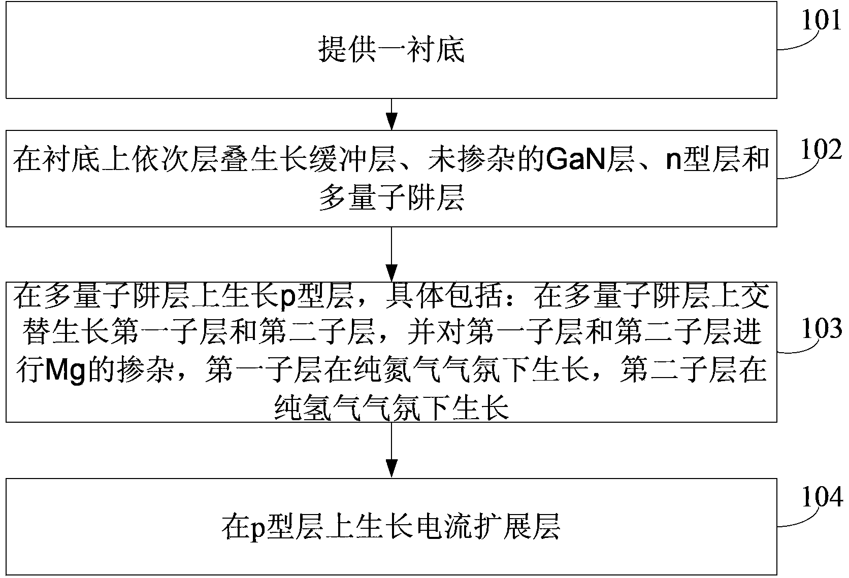
[0026] An embodiment of the present invention provides a method for growing a GaN-based light-emitting diode chip, see figure 1 , the method includes:

[0027] Step 101: Provide a substrate.

[0028] Specifically, in this embodiment, the substrate may be a sapphire substrate.

[0029] Step 102: stacking a growth buffer layer, an undoped GaN layer, an n-type layer and a multi-quantum well layer sequentially on the substrate.

[0030] Optionally, in this embodiment, the n-type layer may be a GaN layer doped with Si.

[0031] Optionally, in this embodiment, the multi-quantum well layer is formed by alternately stacking InGaN layers and GaN layers in sequence. When growing multiple quantum well layers, since In is very sensitive to temperature and easily volatilizes at high temperatures, in order to facilitate the growth of In, the growth temperature of the InGaN layer should be lower, and the GaN layer requires better crystal quality and a higher temperature,...


PUM

PropertyMeasurementUnit
Thicknessaaaaaaaaaa

Abstract

The invention discloses a GaN-base light-emitting diode chip growing method and belongs to the technical field of semiconductors. The method comprises the steps that a substrate is provided; a buffering layer, an undoped GaN layer, an n-type layer and a multiple-quantum-well layer grow on the substrate in sequence in an overlapping mode; a p-type layer and a current expanding layer grow on the multiple-quantum-well layer; the p-type layer grows on the multiple-quantum-well layer. Specifically, the GaN-base light-emitting diode chip growing method comprises the steps that a first sub-layer and a second sub-layer grow on the multiple-quantum-well layer in an alternating mode, Mg doping is carried out on the first sub-layer and the second sub-layer, the first sub-layer grows in a pure-nitrogen atmosphere, and the second sub-layer grows in a pure-hydrogen atmosphere. According to the method, the first sub-layer grows in the pure-nitrogen atmosphere, doped Mg activation can be well improved, Mg activation can improve hole concentration; the second sub-layer grows in the pure-hydrogen atmosphere, due to the strong reducing property of hydrogen, impurities in crystals can be reduced, the injection efficiency of holes is increased, and crystal quality and chip light-emitting efficiency are improved.

Description

technical field [0001] The invention relates to the technical field of semiconductors, in particular to a method for growing a GaN-based light-emitting diode chip. Background technique [0002] Today's GaN-based light-emitting diodes have been used in various fields such as display screens, backlight sources, traffic lights, landscape lights, and lighting. GaN-based light-emitting diode chips are the core components of GaN-based light-emitting diodes. [0003] Existing GaN-based light-emitting diode chips generally adopt heterogeneous epitaxial growth methods. Due to the mismatch of lattice constants and thermal expansion coefficients between materials, a large number of dislocations and defects will be generated, and multi-quantum well layers are generally grown at relatively low temperatures. , and its lower growth temperature will also produce a large number of dislocations and defects, which will extend to the p-type layer and affect the crystal quality of the p-type la...

Claims


Application Information

Patent Timeline
IPC IPC(8): H01L33/02H01L33/00
CPCH01L21/0254H01L21/02579H01L33/0075
Inventor 杨兰魏世祯胡加辉
Owner HC SEMITEK CORP
Why Eureka
Try Eureka