Resistive random access memory with high uniformity and manufacturing method thereof

A resistive memory and consistency technology, applied in static memory, digital memory information, information storage, etc., can solve the problems of increasing process complexity and difficulty in operation, and achieve the advantages of process integration, simple process steps, and easy implementation. Effect

Inactive Publication Date: 2014-01-15
PEKING UNIV
View PDF8 Cites 9 Cited by
  • Summary
  • Abstract
  • Description
  • Claims
  • Application Information

AI Technical Summary

Problems solved by technology

[0007] Both of the above two invention patent applications generate peak-shaped grooves through the anisotropy of etching. This process method strongly relies on etching technology. In actual operation, the etching conditions must be carefully and strictly controlled, which is difficult to operate and increases process complexity

Method used


Image

  • Resistive random access memory with high uniformity and manufacturing method thereof
  • Resistive random access memory with high uniformity and manufacturing method thereof
  • Resistive random access memory with high uniformity and manufacturing method thereof

Examples


Embodiment Construction

[0043] Below in conjunction with accompanying drawing and specific embodiment the present invention is described in further detail:

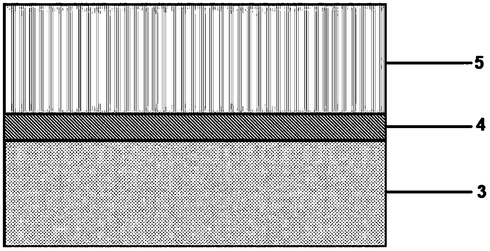
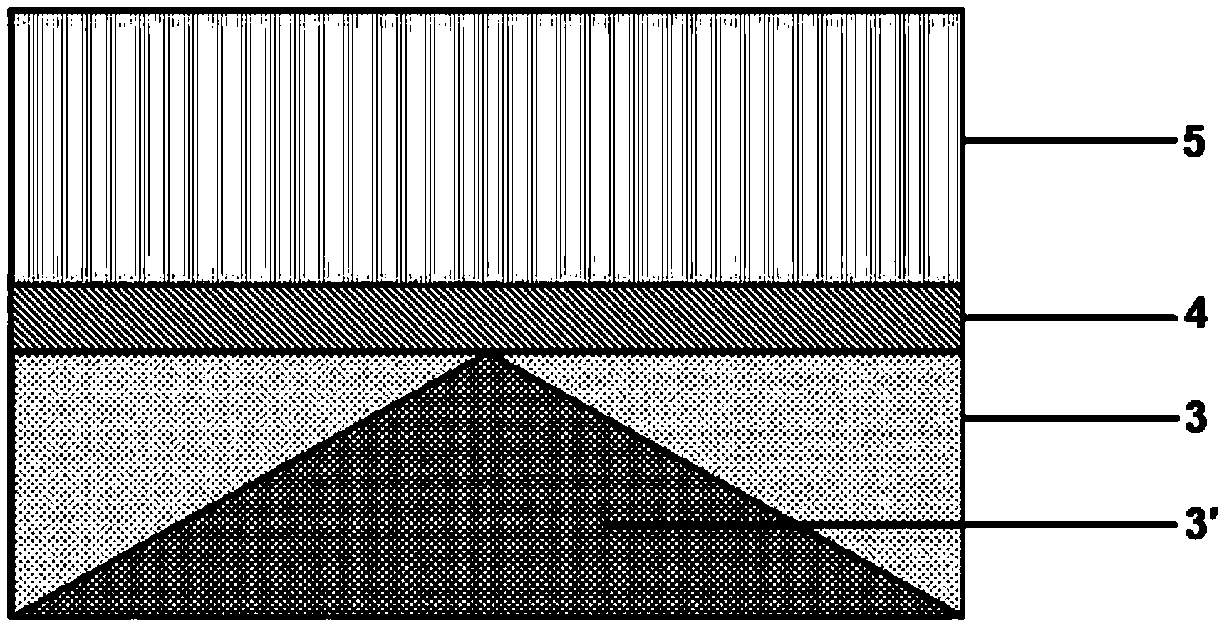
[0044] The resistive variable memory with high consistency of the present invention has a main structure such as figure 2 As shown, it includes a bottom electrode 3, a heavily doped peak region 3′, a resistive material thin film 4 and a top electrode 5, which are consistent with the mainstream resistive memory structure ( figure 1 ) is that the bottom electrode 3 uses a selectively heavily doped silicon substrate, and its heavily doped region forms a peak-like structure, so that the electric field is concentrated, and the resistive switching behavior occurs controllably at the peak.

[0045] The process of preparing the high-consistency RRAM according to the present invention is described as follows in conjunction with the accompanying drawings:

[0046] 1) Prepare the substrate. Select the substrate 1 opposite to the heavily doped polarity, ...


PUM


Abstract

The invention discloses a resistive random access memory with high uniformity and a manufacturing method thereof. A method that a graphical area of substrate silicon is used as a bottom electrode to be combined with selective heavy doping is adopted, and a proper ion injection direction is selected, so that an electric field can be controllably concentrated within a partial peak range, operation in every time and resistive random action of each element occur in the same position, and uniformity of the elements is effectively improved. According to the resistive random access memory and the method, a simple process method is used, the resistive random access memory with high uniformity can be manufactured, and meanwhile the electrode is avoided from being made of precious metal Pt, and process integration is facilitated.

Description

technical field [0001] The present invention relates to a resistive memory (RRAM), in particular to a design scheme of a highly consistent resistive memory and a preparation method thereof, belonging to the performance optimization of nonvolatile memory (Nonvolatile ememory) in CMOS ultra-large-scale integration (ULSI) and its field of manufacturing technology. Background technique [0002] With the continuous advancement of microelectronics technology to nanoelectronics, how to deal with various problems caused by size reduction has become the key to the development of semiconductor technology. As far as the memory field is concerned, after entering the nanometer size node, the shrinking capabilities of the current mainstream memories, namely DRAM, SRAM and Flash, will reach their limits. In particular, the random fluctuation of parameters such as the performance of non-volatile memory has increased significantly, and the reliability problem has become increasingly severe....

Claims


Application Information

Patent Timeline
Patent Type & Authority Applications(China)
IPC IPC(8): H01L45/00G11C13/00
Inventor 黄如余牧溪蔡一茂方亦陈潘越黎明
Owner PEKING UNIV
Why Eureka
Try Eureka