Low-igniting-voltage miniature semiconductor bridge igniting assembly

A semi-conductor and low-ignition technology, applied in weapon accessories, blasting barrels, fuzes, etc., can solve the problems of poor charge resistance and poor electromagnetic safety, and achieve the effect of reducing ignition energy, high safety current and rapid action

Inactive Publication Date: 2015-07-08
BEIJING INSTITUTE OF TECHNOLOGYGY
View PDF2 Cites 0 Cited by
  • Summary
  • Abstract
  • Description
  • Claims
  • Application Information

AI Technical Summary

Problems solved by technology

Grooves cannot be made on the glass plug, and the semiconductor bridge chip can only be fixed on the surface of the glass plug, which will deteriorate the pressure resistance of the charge, so it is rarely used
[0006] In Chapter 4 of Yang Guili's dissertation "Study on Energy Conversion and Ignition Laws of Micro-Semiconductor Bridges" in 2010, she pointed out that for the current low-energy excitation (below 5V) bridge-wire EEDs in my country, the safety current is not greater than 50mA. For the hidden danger of poor safety, the size of the semiconductor bridge is miniaturized. By reducing the volume and energy of the bridge heated by the electric thermal explosion, the volume and ignition energy of the bridge are much smaller than the conventional size of the insensitive semiconductor bridge.
It is undoubtedly a huge challenge to rely on the technical level of the existing EPD design for such a combination of size and ignition performance parameters.

Method used


Image

  • Low-igniting-voltage miniature semiconductor bridge igniting assembly
  • Low-igniting-voltage miniature semiconductor bridge igniting assembly
  • Low-igniting-voltage miniature semiconductor bridge igniting assembly

Examples


Embodiment

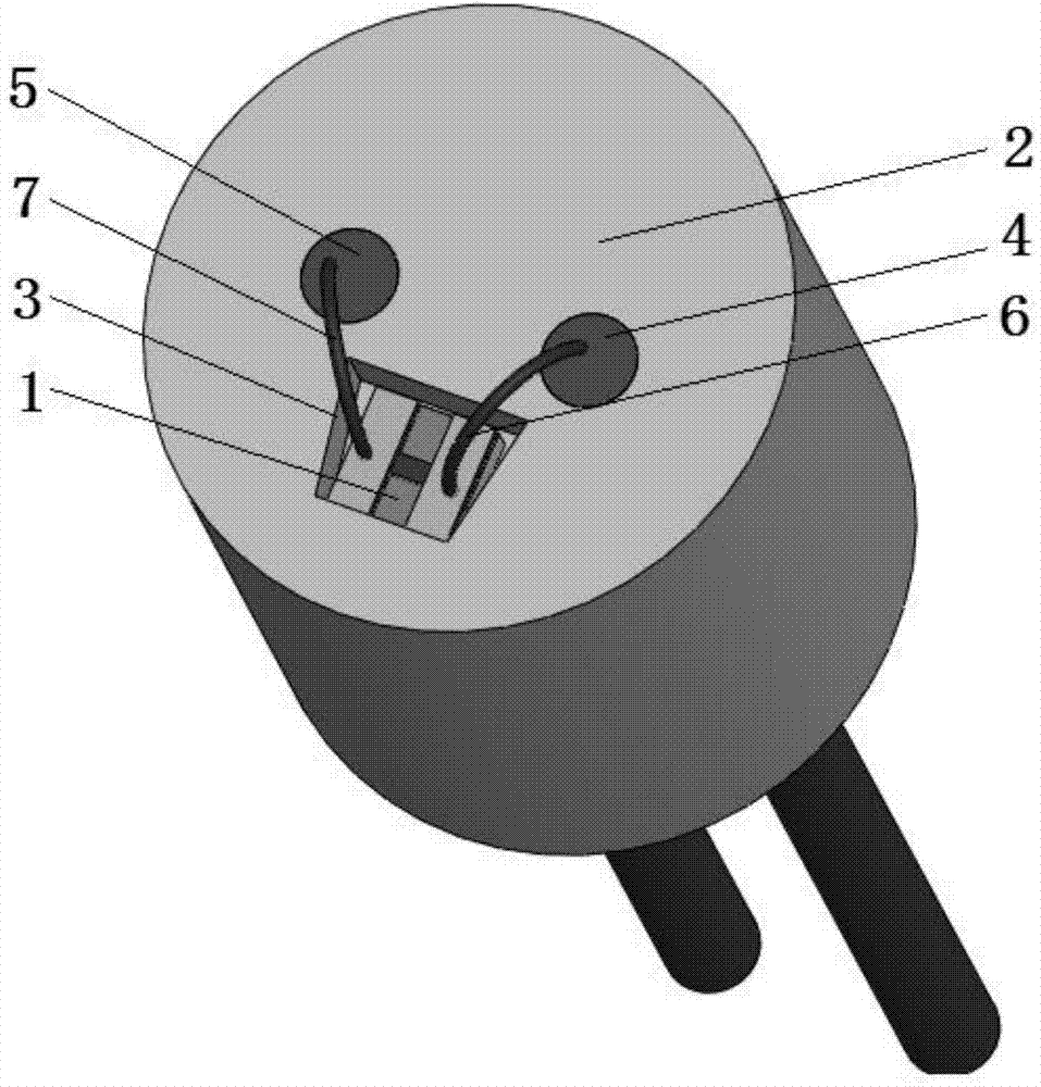
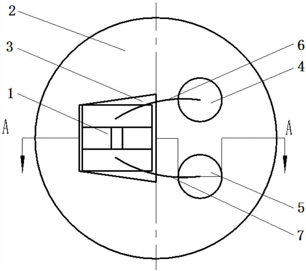
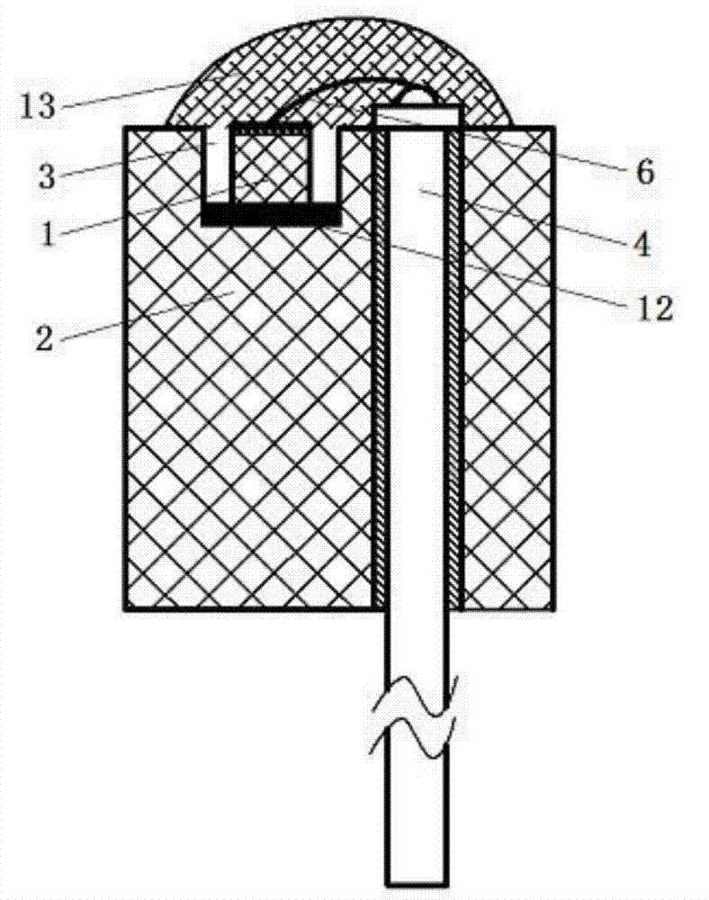
[0023] Embodiment: The substrate of the semiconductor bridge transducer chip is monocrystalline silicon, which is first oxidized into a silicon dioxide layer with a thickness of 0.2 μm on the monocrystalline silicon, and a layer of polycrystalline silicon with a thickness of 2 μm is deposited by vapor deposition, and then doped with P Atoms, the doping concentration is 7.7×10¹⁹ / cm3, and then a rectangular pattern is etched through a mask, and finally two metal pads are evaporated with a thickness of 0.2 μm for external circuit connection. The pad material is aluminum or Gold, and then mask the required pattern by photolithography, and obtain a single semiconductor bridge transducer chip by scribing. The side length of the semiconductor bridge transducer chip is 0.5mm, the height is 0.6mm, and the bridge area is 20 μm in length and 20 μm in width. is 50μm, and the resistance is 3.5Ω.

[0024] Adhesive for a rectangular semiconductor bridge transducer chip (1) with a length of 1...


PUM


Abstract

The invention discloses a low-igniting-voltage miniature semiconductor bridge igniting assembly. According to the low-igniting-voltage miniature semiconductor bridge igniting assembly, a semiconductor bridge transduction element chip is fixed in a trapezoid groove of a miniature unsymmetrical ceramic electrode plug through bonding agents, two metal electrode bonding pads on the semiconductor bridge transduction element chip are connected with two leg wire electrodes of the ceramic electrode plug respectively in a welding mode through bonding metal wires, two leg wires and a semiconductor bridge are in circuit connection, and the position above a semiconductor bridge transduction element is filled with electric heating sensitive igniting powder. The minimum full igniting voltage of the low-igniting-voltage miniature semiconductor bridge igniting assembly is as low as 3.83V(10 microfarads), the minimum full igniting energy is 0.074mJ, the safe current is not smaller than 200mA, the igniting time is 12.6-16.5 microseconds, the low-igniting-voltage miniature semiconductor bridge igniting assembly has the advantages of being low in igniting energy, short in action time, good in effect consistency and good in antistatic and radio frequency resistant capacity, and the low-igniting-voltage miniature semiconductor bridge igniting assembly is suitable for application prospects of micro electro mechanical systems.

Description

Technical field [0001] The patent of the present invention relates to a semiconductor bridge ignition device, especially a semiconductor bridge ignition device capable of reliable ignition under low ignition voltage input conditions and miniaturized volume. Background technique [0002] The semiconductor bridge ignition part is generally composed of a semiconductor bridge transducer chip, a substrate or an electrode plug for fixing the transducer chip, foot wires, bonding metal wires, energetic materials and a packaging shell. When the ignition current or voltage is input, heat will be generated when the current passes through the energy-converting element of the semiconductor bridge, and the energetic material will be ignited. By adjusting the semiconductor bridge material, doping concentration, bridge area, thickness, substrate heat dissipation performance and structure, packaging structure, electrostatic discharge structure, ignition performance of energetic materials, ma...

Claims


Application Information

Patent Timeline
Patent Type & Authority Patents(China)
IPC IPC(8): F42B3/13F42C19/12
Inventor 严楠王刚鲍丙亮何爱军焦清介叶耀坤娄文忠张威刘登程温玉全
Owner BEIJING INSTITUTE OF TECHNOLOGYGY
Why Eureka
Try Eureka