
A method for depositing polysilicon by lpcvd

A polysilicon, deposition temperature technology, applied in polycrystalline material growth, chemical instruments and methods, crystal growth, etc., can solve the bipolar circuit compatibility can not meet the needs of the application, the maintenance cycle slows down the production capacity of the semiconductor process, and can not eliminate defects impact and other issues, to achieve the effect of improving production efficiency, increasing maintenance cycle, and increasing deposition quality

Active Publication Date: 2016-05-11
CSMC TECH FAB2 CO LTD
View PDF2 Cites 0 Cited by
  • Summary
  • Abstract
  • Description
  • Claims
  • Application Information

AI Technical Summary

Problems solved by technology

[0002] In the early 1960s, the aluminum gate MOSFET was produced in the early stage. Its speed, integration, power supply voltage, and compatibility with bipolar circuits could no longer meet the needs of applications. Therefore, polysilicon films were used as self-aligned insulated gate field effect Gate and interconnect materials for transistors
[0006] However, the cleaning and maintenance of the inner tube cannot prevent the adverse effects of the particles on the tube wall on the deposition process.
At the same time, frequent maintenance cycles also slow down the production capacity of the entire semiconductor process

Method used

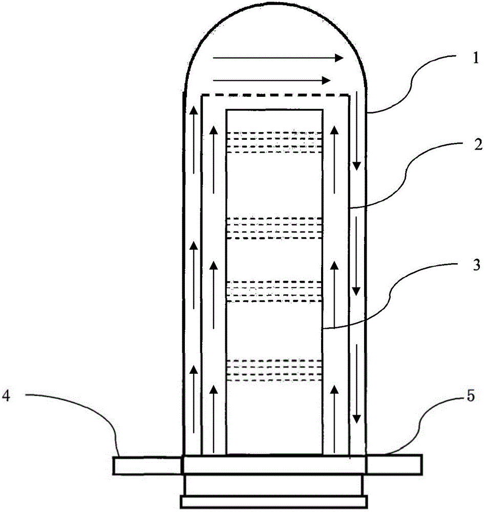

Image

  • A method for depositing polysilicon by lpcvd
  • A method for depositing polysilicon by lpcvd
  • A method for depositing polysilicon by lpcvd

Examples


Embodiment Construction

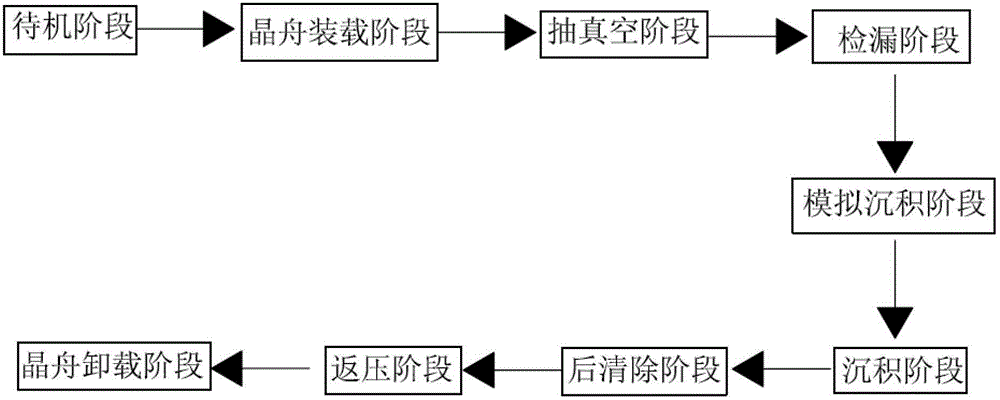
[0022] In order to clearly illustrate the improvement of the present invention, it is necessary to briefly introduce the existing LPCVD process. See figure 2 , figure 2 It is the existing LPCVD process flow chart. As shown in the figure, a deposition process is divided into the following stages: standby stage, crystal boat loading stage, vacuuming stage, leak detection stage, simulated deposition stage, and deposition stage , post purge phase, back pressure phase and wafer boat unloading phase. In the above-mentioned stages, considering the stability of the process, the temperature is set to be constant, that is, the temperature in the inner tube is the same temperature from the beginning to the end of the standby stage. What is changed is the pressure parameter of the inner tube and the flow rate and type of the gas.

[0023] The inventor's research has found that the existing LPCVD can easily lead to the deposition of particles on the inner tube wall for the following r...


PUM


Abstract

The invention discloses an LPCVD (Low Pressure Chemical Vapor Deposition) method of polycrystalline silicon. According to the method, deposited particulate matters on a tube wall can fall off during temperature change through carrying out staged heating before deposition and staged cooling after deposition; then, the particulate matters cannot pollute the surfaces of wafers by using synchronous nitrogen gas purging, so that the quality of polycrystalline silicon film deposition is improved; meanwhile, accumulated deposited particulate matters of an inner tube during single deposition are reduced, the maintenance cycle for the inner tube is prolonged, so that the production efficiency is increased.

Description

technical field [0001] The invention discloses a method for producing polysilicon, which belongs to the field of semiconductor manufacturing, in particular to a method for producing polysilicon by using a low-pressure chemical vapor deposition process. Background technique [0002] In the early 1960s, the aluminum gate MOSFET was produced in the early stage. Its speed, integration, power supply voltage, and compatibility with bipolar circuits could no longer meet the needs of applications. Therefore, polysilicon films were used as self-aligned insulated gate field effect Gate and interconnect materials for transistors. With the development of integrated circuits, the application of polysilicon is becoming wider and wider, such as for differential oxidation to simplify the process flow; for load resistors to shrink circuit units, and so on. [0003] Among various methods of making polysilicon, Low Pressure Chemical Vapor Deposition (LPCVD for short) has become the most commo...

Claims


Application Information

Patent Timeline
Patent Type & Authority Patents(China)
IPC IPC(8): C23C16/44C23C16/24C30B28/14C30B29/06
Inventor 权昊
Owner CSMC TECH FAB2 CO LTD
Learn More