

Thin film transistor and producing method
A technology of thin film transistor and manufacturing method, which is applied in the direction of transistor, semiconductor/solid-state device manufacturing, semiconductor device, etc., can solve the problems of component failure and leakage current, etc.
- Summary
- Abstract
- Description
- Claims
- Application Information
AI Technical Summary
Problems solved by technology
Method used
Image

Examples
Embodiment Construction
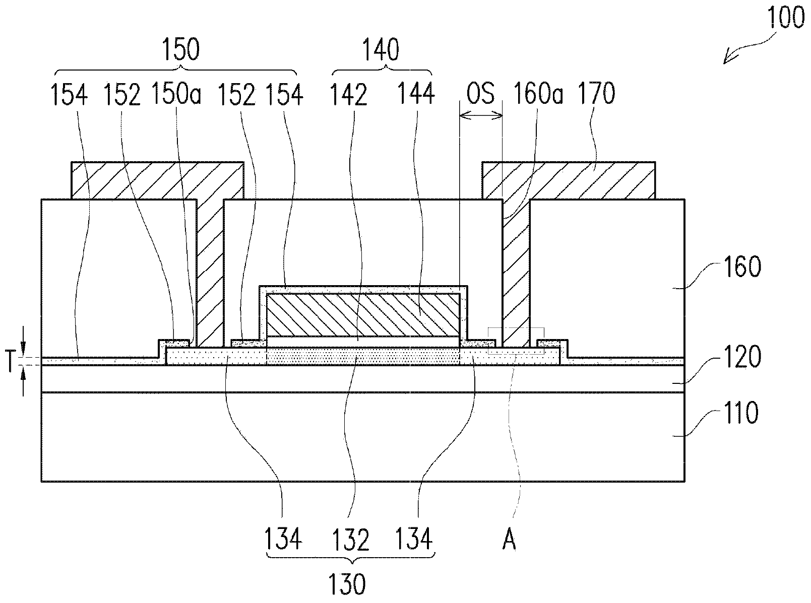
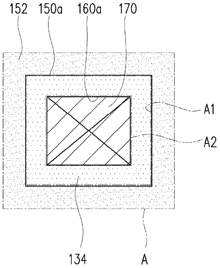
[0039] figure 1 is a schematic cross-sectional view of a thin film transistor 100 according to the first embodiment of the present invention, and figure 2 yes figure 1 A schematic top view of area A in , wherein the area A is the area of one of the first openings.
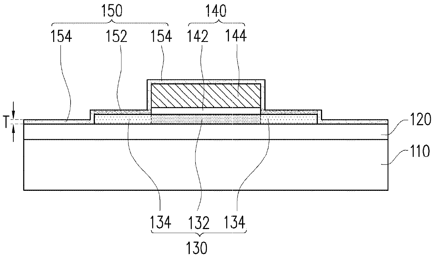
[0040] The thin film transistor 100 is disposed on a substrate 110 . The material of the substrate 110 is, for example, glass, quartz, organic polymer or metal. Furthermore, in this embodiment, the buffer layer 120 is disposed between the thin film transistor 100 and the substrate 110 , that is, the buffer layer 120 may be disposed on the substrate 110 . The material of the buffer layer 120 is, for example, oxide. However, the present invention is not limited thereto. In other embodiments of the present invention, the buffer layer 120 may not be included, as long as the substrate 110 can withstand the photolithography and etching process in the manufacturing method of the thin film transistor 100 .
[0041...
PUM
 Abstract
Description
Claims
Application Information