Method for manufacturing microwave thin film attenuator

A technology of a microwave thin film and a manufacturing method, which is applied to waveguide-type devices, electrical components, circuits, etc., can solve the problems of difficult control and realization of wrapping grounding, poor grounding effect, and low production efficiency, and is conducive to miniaturization and processing. High efficiency and beneficial to mass production

Inactive Publication Date: 2014-01-29
THE 41ST INST OF CHINA ELECTRONICS TECH GRP
View PDF5 Cites 11 Cited by
  • Summary
  • Abstract
  • Description
  • Claims
  • Application Information

AI Technical Summary

Problems solved by technology

[0003] The product in the prior art mainly has the defective of two aspects: 1, adopt thick film attenuator
Although thin-film attenuators can realize fine circuit patterns and meet the occasions of high-frequency applications, the wrapping of the ground electrode is an extremely heavy work, with low efficiency and high cost, which is very unfavorable for mass production
Especially for miniaturized attenuators (<1mm2), wrapping grounding becomes difficult to control and realize
Most of the products on the market put the grounding electrode in the subsequent assembly process. The grounding electrode is realized by bonding gold wire or side-wrapped gold belt or gold mesh. The production efficiency is low, the use is inconvenient, and the grounding effect is not good.

Method used


Image

  • Method for manufacturing microwave thin film attenuator
  • Method for manufacturing microwave thin film attenuator
  • Method for manufacturing microwave thin film attenuator

Examples


Embodiment Construction

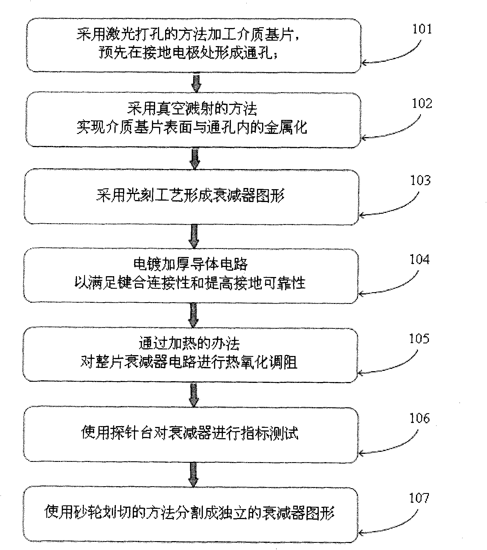
[0037] Such as figure 1 Shown as a specific embodiment of the present invention, the manufacturing method of the microwave thin film attenuator mainly includes the following steps:

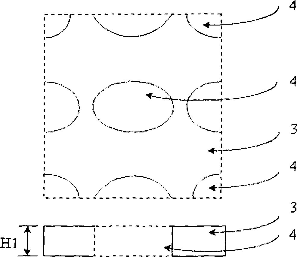
[0038] Step 101: Process the dielectric substrate by laser cutting, and form through holes in the ground electrode in advance;

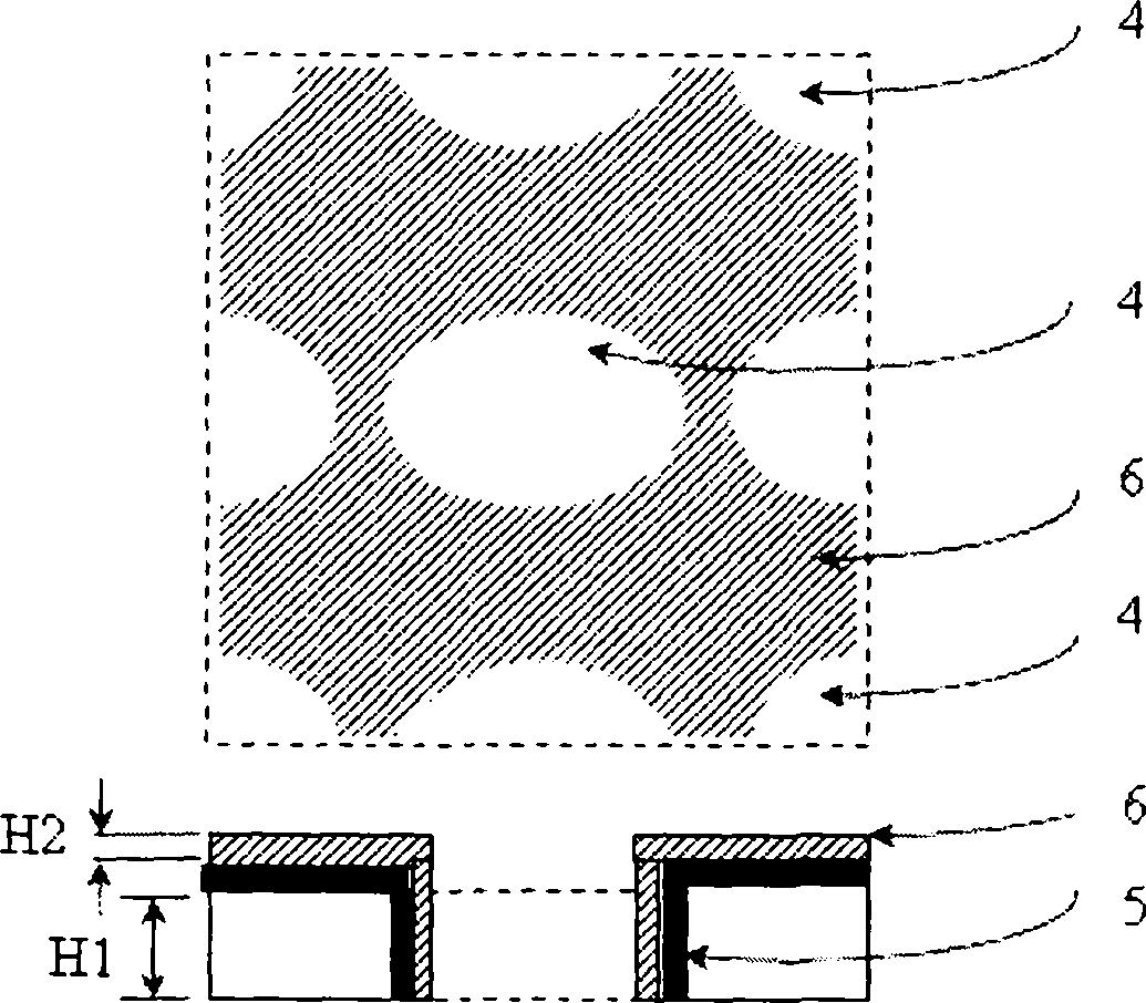
[0039] Step 102: Use a vacuum sputtering method to realize metallization on the surface of the dielectric substrate and the through hole;

[0040] Step 103: Use a photolithography process to form an attenuator pattern;

[0041] Step 104: Plating a thickened conductor circuit to satisfy bonding connectivity and improve grounding reliability;

[0042] Step 105: Perform thermal oxidation resistance adjustment on the entire attenuator circuit by heating;

[0043] Step 106: Use the probe station to perform index test on the attenuator;

[0044] Step 107: Use a dicing method to divide into independent attenuator patterns, and reflect the side metalization effect on the four corners of the...


PUM

PropertyMeasurementUnit
thicknessaaaaaaaaaa
wavelengthaaaaaaaaaa
thicknessaaaaaaaaaa

Abstract

The invention belongs to the technical field of attenuators and relates to a method for manufacturing a microwave thin film attenuator. The method comprises the steps that a medium substrate is processed through a laser cutting method, and a through hole is formed in the position of a grounding electrode; metallization of the surface of the medium substrate and the inside of through hole is achieved through a vacuum sputtering method, and a metallized film layer structure is formed; a attenuator diagram is formed through the photolithography technique; a conductor circuit is thickened through electroplating; thermal oxidation resistance adjustment is conducted on the whole piece of attenuator through a heating method, a probe station is utilized to conduct index testing on the attenuator; independent attenuator diagrams are formed in a cutting method, and the lateral metallization effect is presented on the four corners of the attenuator. The method for manufacturing the microwave thin film attenuator can achieve the fine circuit diagrams, is favorable for being minimized, meets the requirements for the occasions of high frequency application, avoids single sheet manual edge wrapping and grounding, improves production efficiency, and is favorable for volume production.

Description

Technical field [0001] The invention relates to a microwave attenuator, in particular to a manufacturing method of a microwave thin film attenuator, and belongs to the technical field of attenuators. Background technique [0002] The attenuator used in the microwave frequency band mainly adopts two transmission line structure forms: one adopts a sling line structure, which is mainly used in microwave components such as programmable step attenuators and coaxial fixed attenuators; the other adopts a microstrip line structure Although it can be packaged separately as a microwave module, it is more used in microwave active components, mainly to achieve the matching between the internal circuits of the components, improve the standing wave ratio of the ports, increase the power of the components, and adjust the amplifier gain. The attenuator of the microstrip line structure is small in size, requires a small standing wave ratio, good attenuation frequency response, and high mutual ind...

Claims


Application Information

Patent Timeline
Patent Type & Authority Applications(China)
IPC IPC(8): H01P11/00H01P1/22
Inventor 马子腾张猛刘金现
Owner THE 41ST INST OF CHINA ELECTRONICS TECH GRP
Why Eureka
Try Eureka