On-chip scratch-pad memory (SPM) management method facing multitasking embedded system

A technology of scratch pad memory and embedded system, which is applied in memory systems, instruments, multi-program devices, etc., and can solve problems such as multi-time, memory block allocation, and insufficient utilization of SPM.

Inactive Publication Date: 2014-02-05
SHANDONG UNIV
View PDF4 Cites 15 Cited by
  • Summary
  • Abstract
  • Description
  • Claims
  • Application Information

AI Technical Summary

Problems solved by technology

However, the current research is mainly focused on the system with only the scratch pad memory SPM, and the use of the scratch pad memory SPM+cache Cache (such as figure 1 ) There are relatively few studies on multitasking systems with storage systems
In the only optimization algorithm for the multi-task system of the scratch pad memory SPM+cache Cache storage system, the algorithm uses functions as the basic allocation unit, and only considers the energy consumption reduction obtained by putting a single function into the SPM. For multi-task systems Inter-task conflicts and conflicts between functions within tasks are not considered, and these conflicts between tasks and within tasks have a great impact on system performance and energy consumption
[0005] Through the tracking research on the execution process of multiple programs, it is found that in many programs, the functions with high access frequency or high cache Cache miss frequency are not necessarily the functions that cause the most inter-task and intra-task conflicts (such as figure 2 , among which the most visited frequency is A 0 and B 1 , the one with the h

Method used


Image

  • On-chip scratch-pad memory (SPM) management method facing multitasking embedded system
  • On-chip scratch-pad memory (SPM) management method facing multitasking embedded system
  • On-chip scratch-pad memory (SPM) management method facing multitasking embedded system

Examples


Embodiment Construction

[0040] An example of the present invention is given below and the present invention will be further described in conjunction with the accompanying drawings.

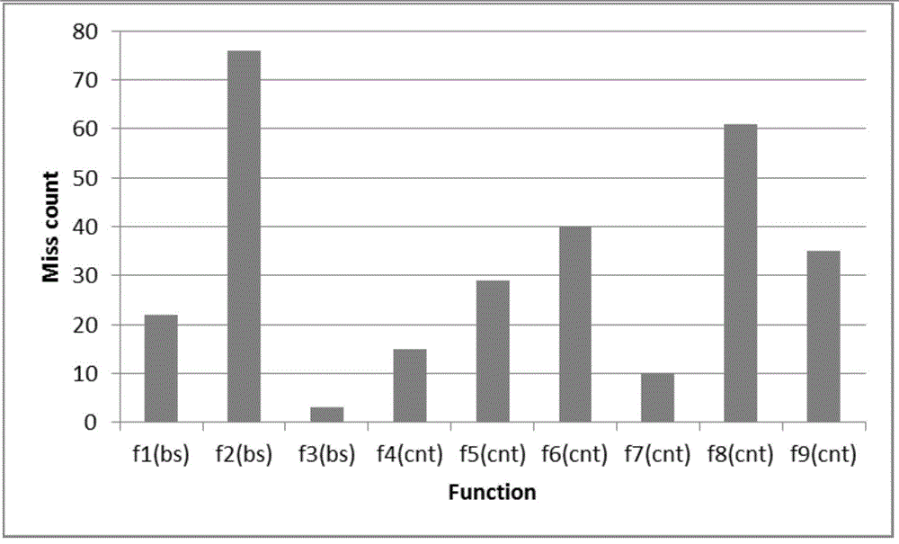
[0041] (1) Pre-analyze the program code segment

[0042] By analyzing the disassembly file, find out the code segment of the source program, and then analyze the program code segment; the analysis of the code segment is to count the first and last address and size of each function of each task in the multi-tasking system, and analyze the multi-tasking system All functions are numbered uniformly. For a task set (including task bs and task cnt) program (such as image 3 , the X-axis is the function number, and the Y-axis is the number of Cache misses) The obtained code segment information is as follows:

[0043] function number

first address

function size

1

4194624

176

2

4194800

88

3

4194888

488

……

……

……

62

4219232

36

[0...


PUM


Abstract

The invention discloses an on-chip scratch-pad memory (SPM) management method facing a multitasking embedded system. The on-chip scratch-pad memory management method comprises the steps as follows: pre-analyzing a program code segment; tracking a program to obtain an internal storage instruction accessing sequence of the program, so as to acquire the accessing times of an internal storage code block and Cache miss information, and accounting and recording a space-time conflict set of the internal storage code block under access of the Cache; selecting an algorithm as required to obtain an optimized SPM distribution scheme; generating a code distribution dispersion loading file, newly mapping and distributing the program code segment, and newly compiling codes to obtain an optimal execution result. Via comprehensive consideration of accessing frequency, cache miss frequency, intertask and intra-task conflict, the required optimal distribution is obtained, the utilization rate of the SPM is maximized, and finally under the premise of ensuring the real-time performance of the program, an optimal execution time scheme or an optimal energy conservation scheme is obtained.

Description

Technical field: [0001] The invention belongs to the field of embedded real-time systems, in particular to an on-chip scratch pad memory management method oriented to multi-task embedded systems. Background technique: [0002] In the development process of embedded systems, since the development speed of the main memory has been much slower than that of the central processing unit, the low reading speed and high energy consumption of the main memory have caused it to become the bottleneck of the performance and energy consumption of many embedded systems. On-chip memory bridges this growing gap between main memory and CPU speed. [0003] In embedded systems, on-chip memory mainly includes two types of scratch pad memory (SPM, Scratch Pad Memory) and cache (Cache). The scratch pad memory SPM and the cache cache are essentially a kind of static random access memory (SRAM, Static Random Access Memory), and the access speed is very fast, close to the speed of the CPU. Cache is...

Claims


Application Information

Patent Timeline
IPC IPC(8): G06F12/08G06F9/50G06F12/0842
CPCY02B60/1225Y02B60/142Y02B60/167Y02D10/00
Inventor 鞠雷贾智平周梓梦
Owner SHANDONG UNIV
Why Eureka
Try Eureka