A kind of flip-chip nano LED chip and preparation method thereof

A LED chip and nanotechnology, applied in semiconductor devices, electrical components, circuits, etc., can solve the problems of ineffective independent electroluminescence, difficult to effectively control the position and size of nanopillars, and leakage, so as to improve light extraction efficiency and reliability , Uniform current expansion, and the effect of reducing leakage current

Active Publication Date: 2016-02-17
PEKING UNIV
View PDF4 Cites 0 Cited by
  • Summary
  • Abstract
  • Description
  • Claims
  • Application Information

AI Technical Summary

Problems solved by technology

[0006] The present invention aims at the problem that the position and size of the nano-pillars are difficult to effectively control in the existing "bottom-up" method for preparing nano-column LEDs, as well as the serious problem of leakage in the "top-down" method and the ineffective independent electroluminescence problem, providing a "top-down" method for fabricating nanopillar LEDs by electron beam exposure and nanoimprinting

Method used


Image

  • A kind of flip-chip nano LED chip and preparation method thereof
  • A kind of flip-chip nano LED chip and preparation method thereof
  • A kind of flip-chip nano LED chip and preparation method thereof

Examples


Embodiment Construction

[0046] The present invention will be further described through the embodiments below in conjunction with the accompanying drawings.

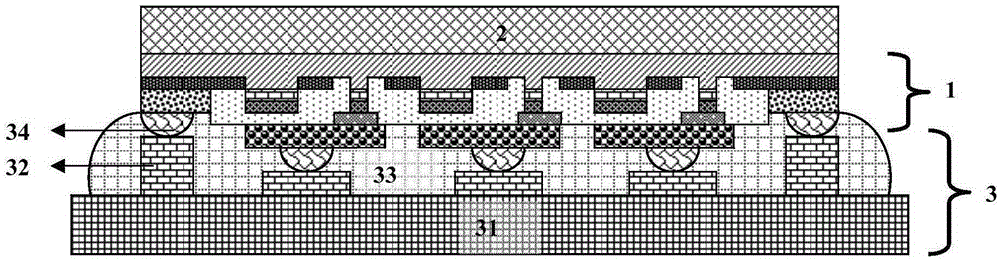
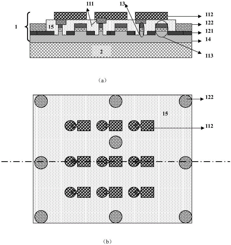
[0047] like figure 1 As shown, the flip-chip nano-LED chip of this embodiment includes: an epitaxial chip part 1, a substrate 2 and a flip-chip soldering part 3; the epitaxial chip part 1 is located on the substrate 2 and includes a p-type contact layer, an n-type contact layer, Nano column array 13, unetched n-type layer 14 and passivation layer 15; P-type contact layer includes p-electrode layer 111, p-pad layer 112 and P-electrode pad platform 113; n-type contact layer includes n-electrode layer 121 And n pad layer 122; Wherein, nanocolumn array 13 is distributed on unetched n-type layer 14; Discrete P electrode pad platform 113 is distributed on unetched n-type layer 14; Nanocolumn array 13 and discrete The p-electrode pads 113 are arranged in a staggered manner; the discrete p-electrode layer 111 corresponds to the nano-pillar array 13 and...


PUM


Abstract

The invention discloses a nano LED flip chip and a manufacturing method thereof. The nano LED flip chip comprises an epitaxial chip part, a substrate and a flip-chip bonding part. The epitaxial chip part located on the substrate is arranged on the flip-chip bonding part in a back-off mode. The manufacturing method achieved from top to bottom is adopted, so that the size and the position of a single nano pillar is effectively controlled, nanoimprinting and electron beam lithography are combined, and a template is used repeatedly so as to facilitate mass production of chips; damage eliminating processing is carried out on the side wall of the nano pillar, so that damages of the side wall are restored, generation of leak currents is reduced, and the function of preventing short circuit is performed; a nano LED chip is combined with a flip-chip structure, so that a device has higher light extraction efficiency, a better heat dissipation effect and more uniform current expansion, and performance of the device is improved; by means of a discrete structure, independent electroluminescence of a single nano LED is achieved, and the current research situation that nano pillar arrays give out light together is changed.

Description

technical field [0001] The invention relates to flip-chip nano-column LEDs, in particular to a nano-LED chip prepared by a top-down method and a preparation method thereof. Background technique [0002] Compared with large-size light-emitting diodes (LEDs), nanocolumn LEDs have many outstanding advantages, such as low dislocation density, and dislocation-free nanocolumn arrays can be obtained by growth methods. Through nanomasks, dry methods or The dislocation density of the wet-etched nanocolumn array will also be reduced by more than two orders of magnitude; the stress release will reduce the quantum confinement Stark effect and increase the radiative recombination effect of the quantum well; the injection efficiency will be improved, and the charge carriers will be transferred through a single nanocolumn. The transmission is limited in one-dimensional structure to obtain high quantum well injection efficiency; it can work with high efficiency under high injection current,...

Claims


Application Information

Patent Timeline
Patent Type & Authority Patents(China)
IPC IPC(8): H01L33/06H01L33/24H01L33/44H01L33/38H01L33/00
CPCH01L33/0075H01L33/06H01L33/38H01L33/44
Inventor 陈志忠焦倩倩姜显哲姜爽李俊泽李顺峰张国义
Owner PEKING UNIV
Why Eureka
Try Eureka