SRAM type FPGA single event upset effect simulation method

A single-event flipping and simulation method technology, applied in the field of SRAM-type FPGA single-event flipping effect simulation, can solve the problems of limited irradiation source conditions, limited ground irradiation test accelerators for aerospace components, etc. Precise results

Active Publication Date: 2014-02-12
CHINA ACADEMY OF SPACE TECHNOLOGY
View PDF3 Cites 36 Cited by
  • Summary
  • Abstract
  • Description
  • Claims
  • Application Information

AI Technical Summary

Problems solved by technology

[0022] The technical problem of the present invention is: to overcome the deficiencies of the prior art, to provide a SRAM-type FPGA single-event flip effect simulation method,

Method used


Image

  • SRAM type FPGA single event upset effect simulation method
  • SRAM type FPGA single event upset effect simulation method
  • SRAM type FPGA single event upset effect simulation method

Examples


Embodiment

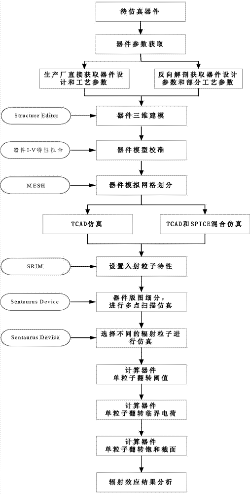
[0062] Step 1: Obtain the design and process parameters of the device to be simulated.

[0063] Enter the detailed process flow and related process parameters and device structure parameters, use the lyt layout information provided by the process manufacturer, and perform process simulation through Sprocess software to obtain device doping information and establish a three-dimensional model of the device; or use the GDS provided by the design unit Layout file, through ICworkbench EV plus software to realize the conversion of GDS file, and obtain the design and process parameters of the simulated device.

[0064] Step 2: Use modeling tools to construct the three-dimensional geometry of the device, and set the doping area, concentration and discretization strategy of the device.

[0065] Step 2.1: Select corresponding process materials for different regions of the device;

[0066] Step 2.2: Design and set process parameters according to the process structure of the transistor. ...

Embodiment 2

[0082] If the unit circuit structure of the simulation device is less than six transistors, the method also needs to go through the specific selection of the following steps in addition to steps 1-4 and steps 6-9 in Embodiment 1:

[0083] Step 1: Use the device-level TCAD simulation method to perform single event effect simulation.

[0084]The device-level three-dimensional model is established one by one for the transistors inside the simulated device. When setting the initial heavy ion incidence, the drain of the TCAD model is connected to a positive potential, the gate is connected to 0, and the source is grounded. Particles with different linear energy transmission values ​​are incident on the sensitive area of ​​the transistor (NMOS drain), and the sensitive node is detected to determine whether a single event flip occurs.

[0085] Taking a certain 300,000-gate SRAM FPGA as an example, the device single-event flip LET threshold obtained by using the method of the present...


PUM


Abstract

Disclosed is an SRAM type FPGA single event upset effect simulation method. The method includes the steps that firstly, design and process parameters of a device to be simulated are acquired; secondly, a three-dimensional geometrical shape of the device is constructed through a modeling tool, and doped areas, doping concentration, discretization strategies and the like of the device are set; thirdly, the design and process parameters of the device are calibrated according to an I-V characteristic curve of the device; fourthly, a meshed device structure is generated, and the mesh is refined on a channel, the light doped area and a PN junction border; fifthly, a device-level TCAD simulation method or a device-level TCAD and circuit-level Spice hybrid simulation method is selected according to the circuit scale and practical conditions of the device; sixthly, characteristics of incident heavy ions are acquired by using a radiating particle characteristic tool to conduct calculation; seventhly, physical model parameters, simulation time, boundary conditions and the like are set, and single event effect simulation of the device is carried out through a TCAD tool; eighthly, particles different in energy are selected to be simulated again according to simulation results; ninthly, the simulation results are acquired through a simulation data analysis tool.

Description

technical field [0001] The invention relates to a simulation method for SRAM-type FPGA single-event flipping effect, belonging to the technical field of anti-radiation of integrated circuits. Background technique [0002] The radiation test can evaluate the radiation resistance of components more accurately, but the radiation test requires special particle accelerator equipment (the simulated heavy ion energy and range are limited, there is no suitable proton accelerator and alpha particle source, etc.), the required It is difficult to guarantee the machine time and the evaluation cost is high. In addition, the radiation test can only be carried out after the components are packaged, and the radiation resistance cannot be evaluated in the design stage of the components. At present, some foreign research institutions such as NASA and ESA have carried out research on radiation effect simulation technology to evaluate the radiation susceptibility of devices. [0003] Componen...

Claims


Application Information

Patent Timeline
IPC IPC(8): G06F17/50
Inventor 祝名张磊罗磊于庆奎孙毅唐民
Owner CHINA ACADEMY OF SPACE TECHNOLOGY
Why Eureka
Try Eureka