
N-bit binary-system electro-optic odd-even checker

A parity check, binary technology, applied in the field of N-bit binary electro-optical parity checker, can solve the problem of small size, achieve the effect of small size, fast check speed and low power consumption

Inactive Publication Date: 2014-02-19
LANZHOU UNIVERSITY
View PDF3 Cites 3 Cited by
  • Summary
  • Abstract
  • Description
  • Claims
  • Application Information

AI Technical Summary

Problems solved by technology

[0004] The present invention is to provide an N-bit binary electro-optic parity checker to solve the bottleneck problems of speed, power consumption, gate delay and competition and risk caused by gate delay in traditional electrical parity checkers. It will play an important role in future photonic communication and computing systems under the premise of keeping the device small size, low power consumption and easy integration

Method used


Image

  • N-bit binary-system electro-optic odd-even checker
  • N-bit binary-system electro-optic odd-even checker
  • N-bit binary-system electro-optic odd-even checker

Examples


Embodiment Construction

[0021] The present invention will be described in further detail below in conjunction with the accompanying drawings and specific embodiments.

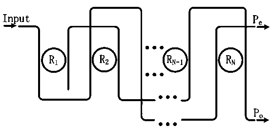
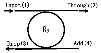
[0022] The N-bit binary electro-optical parity checker of the present invention is composed of N ring waveguides and two curved waveguides, referring to the attached figure 1 , whose basic structure is an MRR-based optical switch, consisting of only one structure of MRR, made of silicon-based nanowire waveguides, N microring resonator MRRs made of semiconductor materials on insulators and two curved Nanowire waveguide implementation, each microring resonator MRR is coupled with two nanowire waveguides, see attached figure 2 . There is a gap or insulation between two adjacent microring resonators MRR that can prevent thermal crosstalk between them.

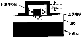
[0023] The MRR structure of the thermal modulation mechanism or electric modulation mechanism of the present invention is shown in image 3 .

[0024] The input of the device of the ...


PUM


Abstract

The invention discloses an odd-even check technology in the technical field of optical communication. An electro-optic odd-even checker is formed by N microring resonators (MRRs) and two bent nanowire waveguides, wherein the MRRs are made of semiconducting material on insulators, each MRR is respectively coupled with the two nanowire waveguides, and a spacer or an insulator is arranged between every two adjacent MRRs and can prevent thermal crosstalk between the two adjacent MRRs. Compared with an electric odd-even checker, the electro-optic odd-even checker has the advantages of being small in size, low in power consumption, high in speed, good in expansibility and capable of being integrated with an electric element conveniently, and has excellent application prospects in an optical communication network.

Description

technical field [0001] The invention relates to the technical field of optical communication, in particular to an N-bit binary electro-optic parity checker, which is especially suitable for future optical communication and optical computing fields. Background technique [0002] With the rapid development of semiconductor technology, the integration of chips or integrated circuits is getting higher and higher, and the CPU can already obtain GHZ-level operating frequency, but the most serious problem brought by high frequency is that the power consumption per unit area of ​​the circuit rises sharply At the same time, due to the further shrinking of the size of integrated components, the leakage and heat dissipation problems cannot be solved well, and the myth of Moore's Law is constantly being challenged. There are various indications that using electrons as information carriers can no longer meet people's requirements for faster processing speeds, while optical communication...

Claims


Application Information

Patent Timeline
IPC IPC(8): H03M13/11
Inventor 田永辉吴小所赵永鹏李德钊杨建红
Owner LANZHOU UNIVERSITY
Learn More