Manufacturing method of low-temperature non-gold ohmic contact of GaN-based high-electronic-mobility transistor
A technology with high electron mobility and ohmic contact, applied in circuits, electrical components, semiconductor devices, etc., to reduce process temperature, reduce manufacturing costs, and avoid pollution
- Summary
- Abstract
- Description
- Claims
- Application Information
AI Technical Summary
Problems solved by technology
Method used
Image

Examples
Embodiment Construction
[0029] In order to make the object, technical solution and advantages of the present invention clearer, the present invention will be described in further detail below in conjunction with specific embodiments and with reference to the accompanying drawings.
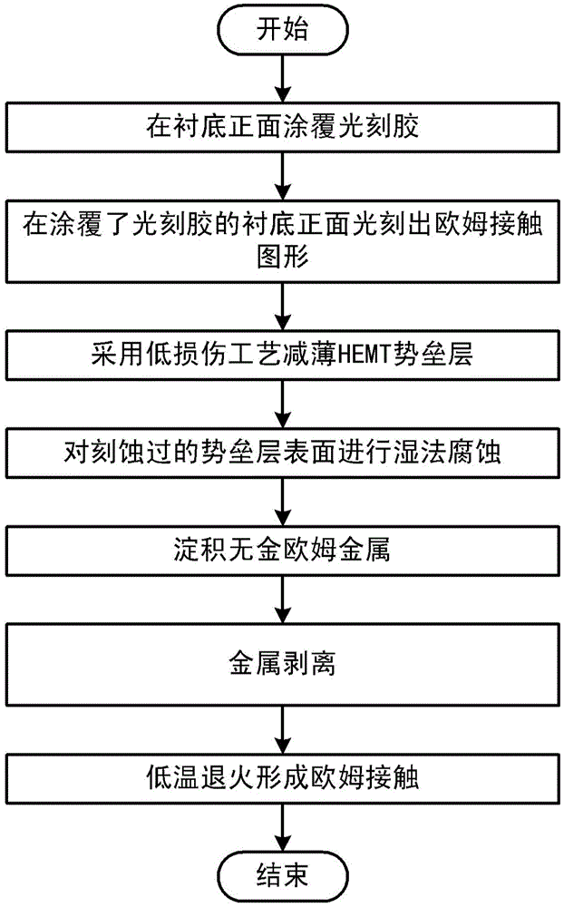
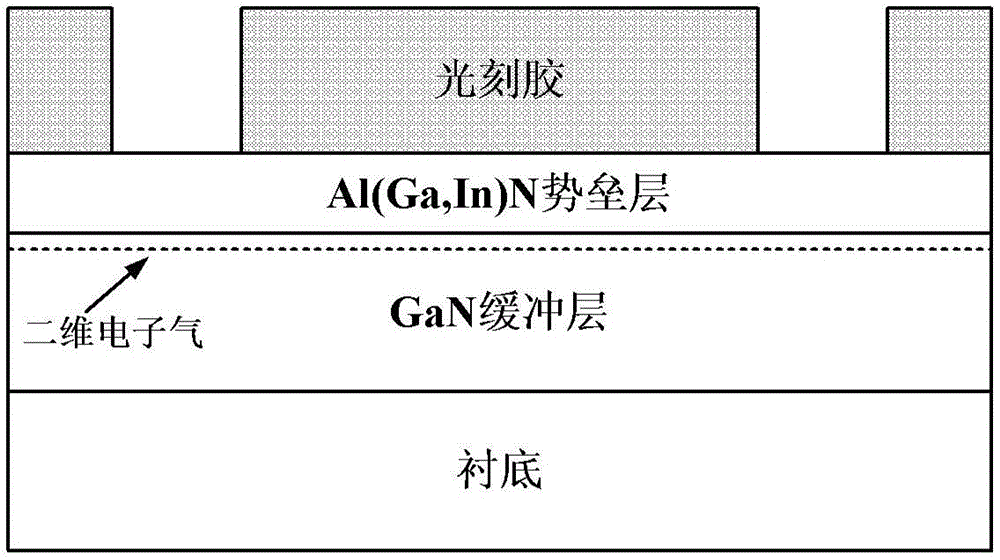
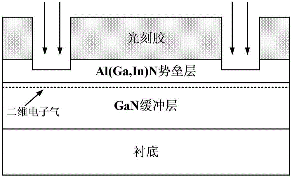
[0030] The fabrication method of the low-temperature gold-free ohmic contact of the GaN-based high electron mobility transistor provided by the present invention is based on the physical property that the tunneling current between the ohmic metal and the two-dimensional electron gas channel increases with the decrease of the distance between the two, through the ohmic The pre-low damage etching process first etches away part of the barrier layer, then deposits gold-free ohmic metal, and anneals at low temperature to form a contact performance comparable to the traditional gold-containing ohmic contact of GaN-based HEMT.
[0031] like figure 1 as shown, figure 1 It is a method for manufacturing a low-temperature gold-free...
PUM
 Abstract
Description
Claims
Application Information
 - R&D
- Intellectual Property
- Life Sciences
- Materials
- Tech Scout
- Unparalleled Data Quality
- Higher Quality Content
- 60% Fewer Hallucinations
Browse by: Latest US Patents, China's latest patents, Technical Efficacy Thesaurus, Application Domain, Technology Topic, Popular Technical Reports.
© 2025 PatSnap. All rights reserved.Legal|Privacy policy|Modern Slavery Act Transparency Statement|Sitemap|About US| Contact US: help@patsnap.com