
Method and device for manufacturing a fiber optic microring resonator

A technology of a micro-ring resonator and a manufacturing method, applied in the field of optical fiber integration, can solve the problems of obstruction, low coupling efficiency, and high production cost, and achieve the effects of simple manufacturing process, improved coupling efficiency, and improved production efficiency

Active Publication Date: 2015-12-09
SICHUAN GUANGSHENG IOT TECH CO LTD
View PDF6 Cites 0 Cited by
  • Summary
  • Abstract
  • Description
  • Claims
  • Application Information

AI Technical Summary

Problems solved by technology

[0004] The microring resonator is mainly composed of a microring resonator cavity and a communication optical fiber, but the preparation of a traditional microring resonator, such as traditional optical etching, nano-molding, trench filling, spin coating, and vacuum evaporation reaction ion The etching method needs to go through a relatively complicated process to form a multi-layer micro-ring resonator, and the final stability is poor, and the production cost is also high, which hinders its development and application to a certain extent. At the same time, because of the connection loss caused by the mismatch between the microring resonator and the communication fiber, the ratio of light transmitted from the microring resonator to the communication fiber, that is, the coupling efficiency, has been difficult to improve. The optical fiber is used as an input / output straight waveguide for optical coupling between the microring resonator to reduce the difficulty of fusion with the communication fiber, but there are large differences between the ordinary optical fiber and the structure and material that constitute the microring resonator, resulting in The coupling efficiency will be very low, and it is difficult to achieve a good resonance effect

Method used


Image

  • Method and device for manufacturing a fiber optic microring resonator
  • Method and device for manufacturing a fiber optic microring resonator
  • Method and device for manufacturing a fiber optic microring resonator

Examples


Embodiment Construction

[0028] The present invention will be further elaborated below in conjunction with the accompanying drawings and specific embodiments.

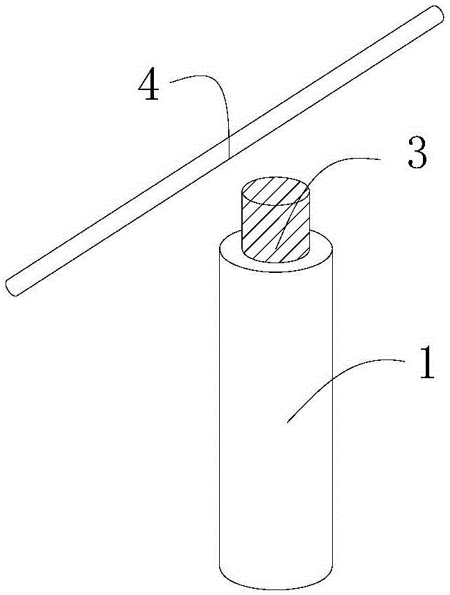
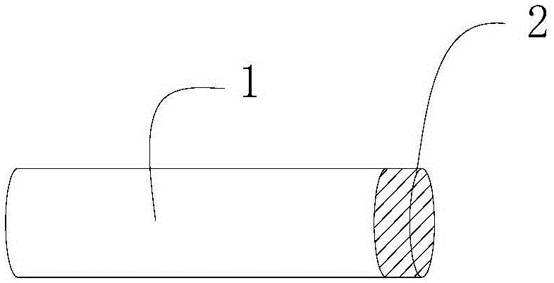
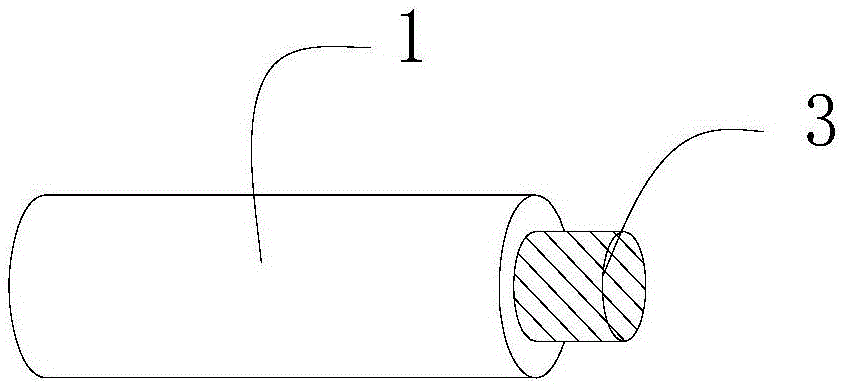
[0029] Such as figure 1 Shown is a schematic diagram of a manufacturing method of an optical fiber microring resonator according to an embodiment of the present invention, which specifically includes the following steps:

[0030] A1. Coating a layer of waveguide material film on the end face of a section of optical fiber;

[0031] The refractive index of the waveguide material film is larger than that of the optical fiber material. The larger the refractive index of the selected waveguide material film is, the smaller the bending loss is. In actual operation, pure silicon film, silicon nitride film and silicon nitride film can be used. film, or a polymer optical waveguide material as the coating material, and silicon nitride material is selected as the coating material in the embodiment of the present invention.

[0032] The specific operati...


PUM


Abstract

The invention discloses a manufacturing method and a device for an optical fiber micro-ring resonator. The specific steps of the method includes: plating a thin film of waveguide material on an end face of a segment of optical fiber; using laser to form a micro ring on a film coating layer of the end face of the optical fiber; using an optical fiber FBT (fused biconical taper) machine to perform fused biconical taper on the other segment of the optical fiber; and making the segment of optical fiber with the micro ring to approach the optical fiber after fused biconical taper, and forming a micro-ring resonator by adjusting the distance between the two segments of optical fiber. According to the manufacturing method for the optical fiber micro-ring resonator, the micro ring is formed in a position of the film coating layer of the end face of the optical fiber, then the optical fiber after being tapered is used to approach the optical fiber with the micro ring to form the micro-ring resonator, the manufacturing process is simple, the coupling gap between the micro ring and a straight waveguide can be adjusted, and thus a relatively small coupling gap can be obtained, thereby improving the coupling efficiency; and laser technology is used to manufacture the micro ring, the dimensional precision of the micro ring that is obtained can reach a micron level, not only is the precision improved, but also the production efficiency can be improved.

Description

technical field [0001] The invention belongs to the technical field of optical fiber integration, and in particular relates to a manufacturing method and device design of an optical fiber microring resonator. Background technique [0002] In the early 1960s, the emergence of ruby ​​lasers and helium-neon lasers opened the prelude to the development of optical communication. Later, with the continuous development of laser technology, optics continued to penetrate and merge with other disciplines, forming many new branches. disciplines or borderline disciplines. In the 1970s, on the basis of the combination of microelectronics and laser technology, integrated optics emerged as a new technology. Its main purpose is to miniaturize the traditional large optical system until it is miniaturized. Instead of simply scaling down the various components that make up the optical system, it is necessary to fundamentally change the structure of these components on the basis of high-tech p...

Claims


Application Information

Patent Timeline
Patent Type & Authority Patents(China)
IPC IPC(8): H01S3/08H01S3/067
Inventor 冉曾令柳珊饶云江王彦君盛龙罗配良
Owner SICHUAN GUANGSHENG IOT TECH CO LTD
Learn More