Formation method for semiconductor structure

A technology of semiconductors and conductive plugs, applied in semiconductor/solid-state device manufacturing, electrical components, circuits, etc., can solve problems such as difficult control and unstable performance of semiconductor devices, achieve stable performance, avoid over-polishing or incomplete polishing, Controllable effect of chemical mechanical polishing process

Active Publication Date: 2014-03-12
SEMICON MFG INT (SHANGHAI) CORP
View PDF6 Cites 4 Cited by
  • Summary
  • Abstract
  • Description
  • Claims
  • Application Information

AI Technical Summary

Problems solved by technology

[0009] However, in the process of forming through-silicon vias in the prior art, the end point of planarization (End Point) is difficult to control, resulting in unstable performance of the formed semiconductor device

Method used


Image

  • Formation method for semiconductor structure
  • Formation method for semiconductor structure
  • Formation method for semiconductor structure

Examples


Embodiment Construction

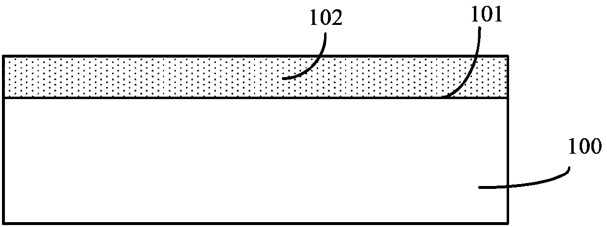
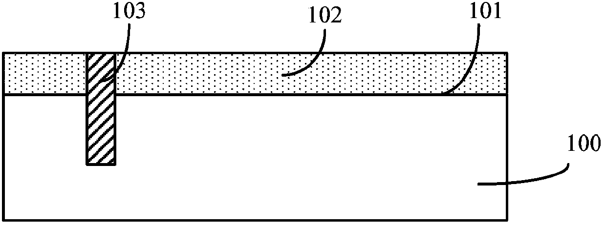
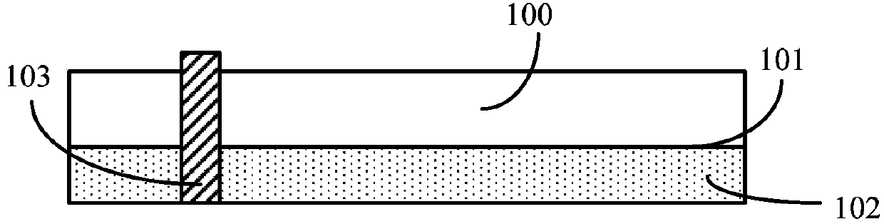
[0031] As mentioned in the background art, in the process of forming through-silicon vias in the prior art, the end point of the planarization is difficult to control, resulting in unstable performance of the formed semiconductor device.

[0032] The inventor of the present invention has discovered through research that the prior art planarizes a silicon substrate 100 (such as image 3 The method of the second surface shown) includes: using a chemical mechanical polishing process to polish the second surface of the silicon substrate until it is close to the conductive plug 103 (such as image 3 As shown); after chemical mechanical polishing, an etching process is used to etch the second surface of the silicon substrate 100 until the conductive plug 103 protrudes from the second surface; however, the position where the chemical mechanical polishing stops It is difficult to control, which will result in over-grinding or incomplete grinding, making it difficult to control the thicknes...


PUM


Abstract

Provided is a formation method for a semiconductor structure. The formation method comprises that: a semiconductor substrate is provided; ion injection is performed on the semiconductor substrate, and a stop layer is formed inside the semiconductor substrate; after the stop layer is formed, a device layer is formed on a first surface of the semiconductor substrate; a conductive plug is formed in the device layer and the semiconductor substrate, wherein the conductive plug is contacted with the stop layer; after the conductive plug is formed, a second surface of the semiconductor substrate is chemically-mechanically polished until the stop layer is exposed, where in the second surface is opposite to the first surface; the stop layer and partial semiconductor substrate are removed so that the conductive plug is protruded out of the second surface of the semiconductor substrate; and after the stop layer and the partial semiconductor substrate are removed, a passivation layer is formed on the second surface of the semiconductor substrate, wherein the surface of the passivation layer is leveled with the top part of the conductive plug. Size of the formed semiconductor device is controllable, and the semiconductor device is stable in performance.

Description

Technical field [0001] The present invention relates to the technical field of semiconductor manufacturing, in particular to a method for forming a semiconductor structure. Background technique [0002] With the continuous development of semiconductor manufacturing technology, the feature size of semiconductor devices continues to decrease, and the integration of chips is getting higher and higher. However, the current two-dimensional packaging structure has been difficult to meet the increasing demand for chip integration, so three-dimensional packaging technology has become a key technology to overcome the bottleneck of chip integration. [0003] Existing three-dimensional packaging technologies include: die stacking based on gold wire bonding, package stacking and three-dimensional stacking based on through silicon vias (TSV). Among them, three-dimensional stacking technology based on through-silicon vias is the main method to improve chip integration. [0004] The three-dimensi...

Claims


Application Information

Patent Timeline
Patent Type & Authority Applications(China)
IPC IPC(8): H01L21/768
CPCH01L21/76841H01L21/76897
Inventor 陈枫周梅生何永根
Owner SEMICON MFG INT (SHANGHAI) CORP
Why Eureka
Try Eureka