InGaN/GaN superlattice buffer layer structure, preparation method of InGaN/GaN superlattice buffer layer structure, and LED chip comprising InGaN/GaN superlattice buffer layer structure

An LED chip and buffer layer technology, applied in the field of multiple quantum wells, can solve the problems of large MQW layer stress in the LED chip, low luminous efficiency of the LED chip, and many crystal defects, so as to improve crystal quality, reduce electron leakage, and improve luminescence. The effect of efficiency

Active Publication Date: 2014-03-12
XIANGNENG HUALEI OPTOELECTRONICS
View PDF4 Cites 16 Cited by
  • Summary
  • Abstract
  • Description
  • Claims
  • Application Information

AI Technical Summary

Problems solved by technology

[0003] The purpose of the present invention is to provide an InGaN/GaN superlattice buffer layer, a preparation method and an LED chip containing the structure, so as to solve the problem

Method used


Image

  • InGaN/GaN superlattice buffer layer structure, preparation method of InGaN/GaN superlattice buffer layer structure, and LED chip comprising InGaN/GaN superlattice buffer layer structure
  • InGaN/GaN superlattice buffer layer structure, preparation method of InGaN/GaN superlattice buffer layer structure, and LED chip comprising InGaN/GaN superlattice buffer layer structure
  • InGaN/GaN superlattice buffer layer structure, preparation method of InGaN/GaN superlattice buffer layer structure, and LED chip comprising InGaN/GaN superlattice buffer layer structure

Examples


Embodiment 1

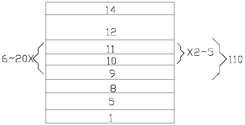
[0047] See structure image 3 .

[0048] 1. Place the sapphire substrate 1 in the MOCVD reaction chamber, and use H 2 , NH 3 Treat the sapphire substrate 1 with the gas at high temperature for 4 to 10 minutes;

[0049] 2. After the treatment is completed, the temperature of the reaction chamber is lowered to 500-550°C, and TMGa and NH 3 , with a pressure of 300-900 mbar, growing a low-temperature first GaN buffer layer 2 (Nucleation) with a thickness of 20-50 nm on the sapphire substrate 1;

[0050] 3. After the first GaN buffer layer 2 is grown, the temperature is raised to 950-1050°C, and the temperature is annealed at a high temperature for 60-300s to form a GaN crystal nucleus on the substrate 1;

[0051] 4. After the high-temperature annealing is completed, the temperature is adjusted to 960-1020°C, and TMGa and NH 3 , the pressure is controlled at 300-900mbar, and a high-temperature non-doped first uGaN layer 3 with a thickness of 0.8-1.2um is grown on the first GaN...

Embodiment 2

[0067] See structure image 3 .

[0068] 1. Place the sapphire substrate 1 in the MOCVD reaction chamber, and use H 2 , NH 3 Treat the sapphire substrate 1 with the gas at high temperature for 4 to 10 minutes;

[0069] 2. After the treatment is completed, the temperature of the reaction chamber is lowered to 500-550°C, and TMGa and NH 3 , with a pressure of 300-900 mbar, growing a low-temperature first GaN buffer layer 2 (Nucleation) with a thickness of 20-50 nm on the sapphire substrate 1;

[0070] 3. After the first GaN buffer layer 2 is grown, the temperature is raised to 950-1050°C, and the temperature is annealed at a high temperature for 60-300s to form a GaN crystal nucleus on the substrate 1;

[0071] 4. After the high-temperature annealing is completed, the temperature is adjusted to 960-1020°C, and TMGa and NH 3 , the pressure is controlled at 300-900mbar, and a high-temperature non-doped first uGaN layer 3 with a thickness of 0.8-1.2um is grown on the first GaN...

Embodiment 3

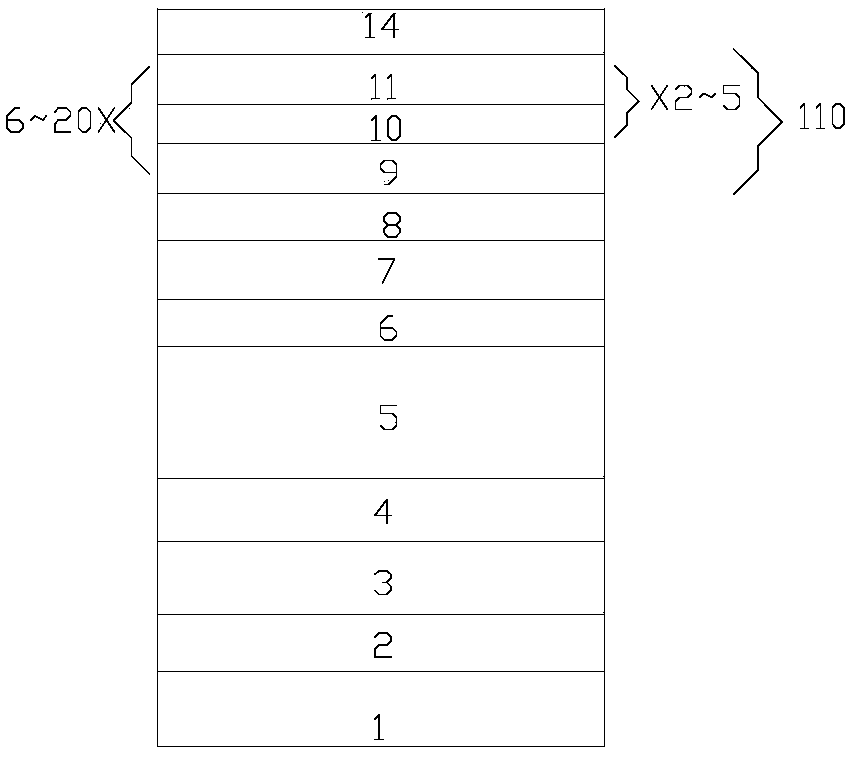
[0087] See structure image 3 .

[0088] 1. Place the sapphire substrate 1 in the MOCVD reaction chamber, and use H 2 , NH 3 Treat the sapphire substrate 1 with the gas at high temperature for 4 to 10 minutes;

[0089] 2. After the treatment is completed, the temperature of the reaction chamber is lowered to 500-550°C, and TMGa and NH 3 , with a pressure of 300-900 mbar, growing a low-temperature first GaN buffer layer 2 (Nucleation) with a thickness of 20-50 nm on the sapphire substrate 1;

[0090] 3. After the first GaN buffer layer 2 is grown, the temperature is raised to 950-1050°C, and the temperature is annealed at a high temperature for 60-300s to form a GaN crystal nucleus on the substrate 1;

[0091] 4. After the high-temperature annealing is completed, the temperature is adjusted to 960-1020°C, and TMGa and NH 3 , the pressure is controlled at 300-900mbar, and a high-temperature non-doped second buffer GaN layer 3 with a thickness of 0.8-1.2um is grown on the fi...


PUM

PropertyMeasurementUnit
Thicknessaaaaaaaaaa
Thicknessaaaaaaaaaa
Thicknessaaaaaaaaaa

Abstract

The invention provides an InGaN/GaN superlattice buffer layer structure, a preparation method of the InGaN/GaN superlattice buffer layer structure, and an LED chip comprising the InGaN/GaN superlattice buffer layer structure. The InGaN/GaN superlattice buffer layer structure comprises a shallow quantum well layer, an MQW layer and a superlattice buffer layer disposed between the shallow quantum well layer and the MQW layer. The superlattice buffer layer comprises a plurality of buffer layer units stacked in order. Each buffer layer unit comprises an InGaN layer and a plurality of doped layers. Each doped layer comprises a uGaN layer and an nGaN layer which are stacked in order. Each doped layer is arranged on the corresponding InGaN layer. The InGaN/GaN superlattice buffer layer structure has the advantages that the quality of active region crystal of the LED chip can be improved, active region lattice mismatch and thermal stress mismatch are reduced, electron leakage is reduced effectively, carriers and holes can be recombined more efficiently, and luminous efficiency of devices is improved.

Description

technical field [0001] The present invention relates to multiple quantum wells, in particular to an InGaN / GaN superlattice buffer layer and a preparation method thereof. Another aspect of the present invention also provides an LED chip containing the structure. Background technique [0002] Most of the existing LED chips grow multiple quantum well (MQW) layers directly on the shallow quantum well layer. The MQW layer includes well layers and barrier layers stacked in sequence. Multi-layer, each layer will generate stress with the previous layer during the growth process, resulting in greater stress in the grown shallow quantum well layer. If the MQW layer is directly grown on the shallow quantum well layer, thermal stress mismatch in the MQW active region will be formed And the quality of the crystal decreases, which increases the number of V-type defects that grow on the MQW layer, increases the electron leakage, is not conducive to the uniform expansion of the current in ...

Claims


Application Information

Patent Timeline
IPC IPC(8): H01L33/12H01L33/06H01L33/00
CPCC30B25/16C30B29/403H01L33/0075H01L33/06H01L33/12
Inventor 马欢
Owner XIANGNENG HUALEI OPTOELECTRONICS
Why Eureka
Try Eureka