In-situ double-axis tilting nanoindenter for transmission electron microscope

A nano-indenter and dual-axis tilting technology, which is applied in the use of radiation for material analysis, etc., can solve the problems of high design cost, limited application range, powerlessness, etc., and achieve reliable performance, expanded functions, and convenient installation.

Inactive Publication Date: 2014-03-19
BEIJING UNIV OF TECH
View PDF9 Cites 9 Cited by
  • Summary
  • Abstract
  • Description
  • Claims
  • Application Information

AI Technical Summary

Problems solved by technology

[0003] At present, many commercial companies and laboratories have invested a lot of manpower and material resources to develop in-situ mechanical performance testing products and have achieved gratifying economic benefits. For example, the 654 mono-tilt tensile sample rod produced by Gatan Company of the United States can realize in-situ in-situ testing of transmission electron microscopy. The stretching operation realizes the research of the structure evolution information under the strain state of the material, but due to the loss of the Y-axis tilt degree of freedom, for crystal materials, it is impossible to realize the evolution information of the microstructure at the atomic scale in situ; in addition, Nanofactory The STM-TEM sample stage produced by the company can realize the deformation operation of materials. However, due to the loss of the Y-axis degree of freedom, it is also difficult to realize the deformation operation at the in-situ atomic scale. The crystal sample just seems powerless, and therefore limits its scope of application
The PI-95 transmission electron microscope sample holder produced by Hysitron Company of the United States can conveniently carry out quantitative nano-indentation and nano-scratch tests, but it also only has the X-axis tilting degree of freedom, and the loss of the Y-axis tilting degree of freedom limits it to a certain extent. Range of application of this sample holder
[0004] It should be pointed out that the above methods have been able to test the mechanical properties of the material under the strain state. Using the above methods, the researchers have achieved very good research results, but because the tilt of the Y axis cannot be realized, so that in The probability of observing the change of the material microstructure at the atomic scale under the positive band axis of the low index is greatly reduced, which is not conducive to the revealing of the evolution mechanism of the atomic scale structure, which brings a huge challenge to people's correct understanding of material strain physics
In addition, because the design cost of this type of sample stage is very high, it is also not conducive to the popularization and promotion of this type of product.

Method used


Image

  • In-situ double-axis tilting nanoindenter for transmission electron microscope
  • In-situ double-axis tilting nanoindenter for transmission electron microscope
  • In-situ double-axis tilting nanoindenter for transmission electron microscope

Examples


specific Embodiment 1

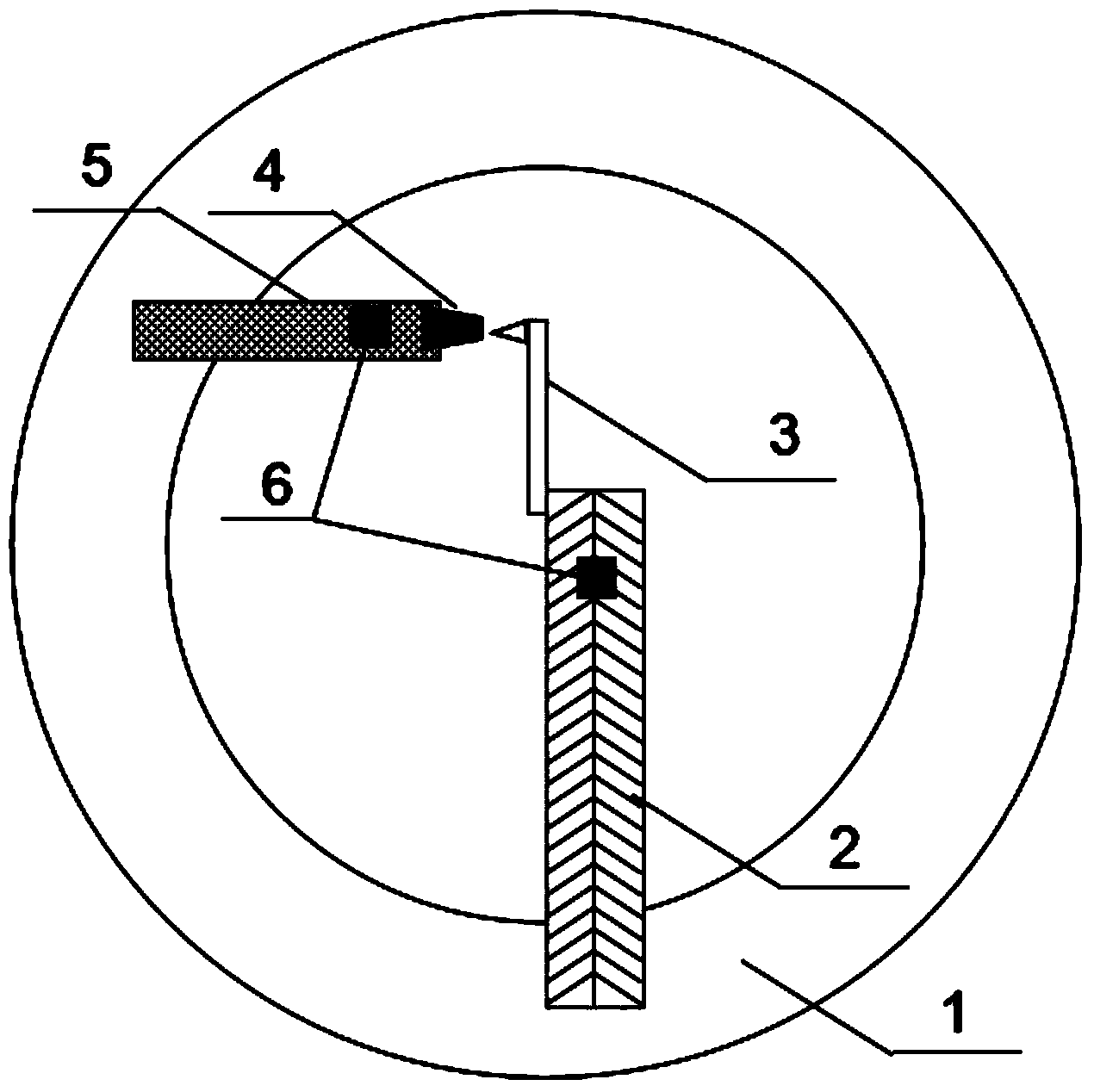
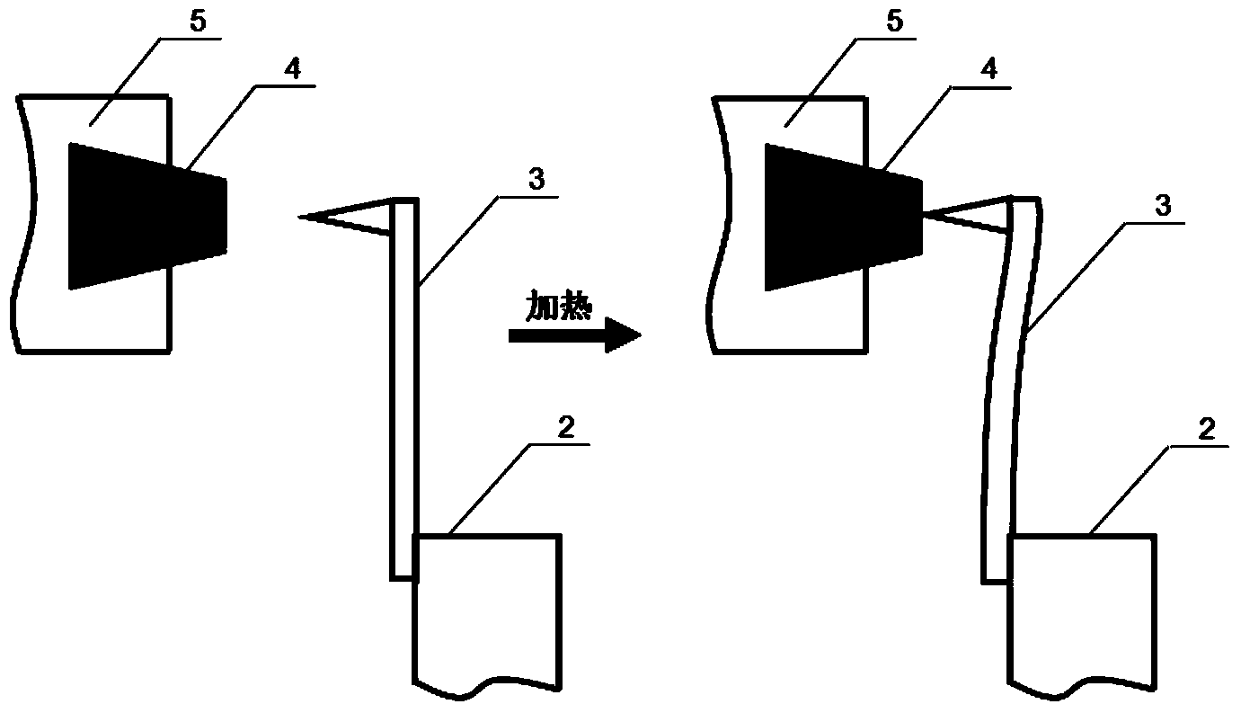
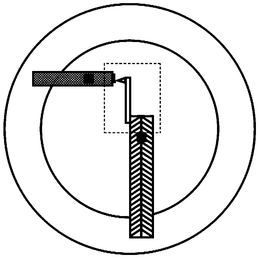
[0031] 1. Press figure 1 As shown, the thermal bimetal is made into a bimetal with a width of 0.2 mm, a thickness of 0.08 mm, and a length of 1.8 mm. At the same time, a Si cantilever needle tip with a length of 0.45 mm, a width of 0.2 mm, a thickness of 0.2 mm, and an elastic coefficient of 0.2 N / m is fixed on the side of the thermal bimetal sheet with a low expansion coefficient, and the unfixed cantilever on the thermal bimetal sheet One side of the beam needle tip is fixed on one side of a copper ring for transmission electron microscopy with an outer diameter of 3.0mm in the middle opening.

[0032] 2. Suspend one section of the thin area of ​​the single crystal Si sample that has undergone mechanical grinding, electrolytic double spraying, and ion thinning, and fix the other end on the sample support platform. Under the optical microscope, fix the sample support platform on the 3mm copper ring, and make The sample is placed directly against the tip of the cantilever bea...


PUM

PropertyMeasurementUnit
thicknessaaaaaaaaaa
widthaaaaaaaaaa

Abstract

The invention provides an in-situ double-axis tilting nanoindenter for a transmission electron microscope and belongs to the nanomaterial in-situ test field. one end of a thermal bimetal sheet is fixed on a metal ring, and the other end is a free end. A cantilever beam needle point is fixed at the free end and one side with a low thermal expansion coefficient. The needle point of the cantilever beam needle point is arranged to be back to the thermal bimetal sheet. A sample is fixed at one end of a sample support. The other end of the sample support is fixed on the metal ring and the sample is arranged to directly face the cantilever beam needle point. The gap between the sample and the needle point is 2-50 micrometers. The thermal bimetal sheet and the cantilever beam needle point, and the sample and the sample support are fixed together through conductive materials respectively. The thermal bimetal sheet and the sample support are fixed on the metal ring respectively in an insulation state. Electrodes are welded on the thermal bimetal sheet and the sample support respectively, and the electrodes are connected with an external test circuit. The nanoindenter keeps two freedom degrees of X axis and Y axis at the same time, and performs real-time in-situ atomic scale observation of structures of nanomaterials during compression.

Description

technical field [0001] The invention relates to an in-situ biaxial tilting nano-indentation device in a transmission electron microscope. The device fixes a force-measuring cantilever beam on a thermal bimetallic sheet, fixes the thermal bimetallic sheet on a copper ring for a transmission electron microscope, and indents nanomaterials with the tip of the cantilever beam by heating the thermal bimetallic sheet. The in-situ image recording system records the deformation of the cantilever beam to obtain mechanical signals, while maintaining the two degrees of freedom of the X and Y axes. While compressing, the transmission electron microscope is used to observe the structure of nanomaterials at the atomic scale in situ in real time. Field of in situ testing methods for nanomaterials. Background technique [0002] With the development of microelectronics and microsystems, many smiling structures have been practically applied. At the same time, the mechanical properties of mat...

Claims


Application Information

Patent Timeline
Patent Type & Authority Applications(China)
IPC IPC(8): G01N23/04
Inventor 韩晓东岳永海张泽
Owner BEIJING UNIV OF TECH
Why Eureka
Try Eureka