Method for improving success rate of transmission electron microscope's irradiation on sample

An electron microscope and success rate technology, which is applied to the use of wave/particle radiation for material analysis, measuring devices, instruments, etc., can solve the problems of inability to carry out transmission electron microscopy, photography, carbon film tilt and distortion, etc., to improve the success rate, Effects of cost reduction and damage rate reduction

Inactive Publication Date: 2014-03-19
SHANGHAI HUALI MICROELECTRONICS CORP
View PDF9 Cites 4 Cited by
  • Summary
  • Abstract
  • Description
  • Claims
  • Application Information

AI Technical Summary

Problems solved by technology

This method solves the problem that the sample with a damaged carbon film is tilted and twisted, which makes it impossible to take pictures with a transmission electron microscope.

Method used


Image

  • Method for improving success rate of transmission electron microscope's irradiation on sample
  • Method for improving success rate of transmission electron microscope's irradiation on sample
  • Method for improving success rate of transmission electron microscope's irradiation on sample

Examples


Embodiment 1

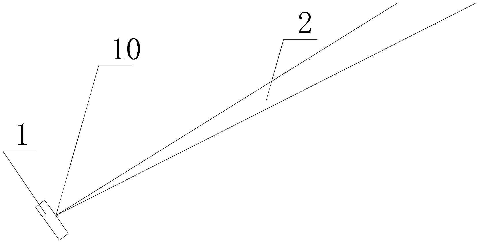
[0032] Since the imaging principle of the transmission electron microscope (not shown in the figure) is that a high-energy electron beam penetrates the sample, the transmitted electrons are focused and amplified, and the detector is used to collect the signal and form an image. Since electrons are easy to scatter and be absorbed by objects, transmission electron microscopy has high requirements for sample preparation, and the requirements for sample thickness vary according to the acceleration voltage, generally around 100nm.

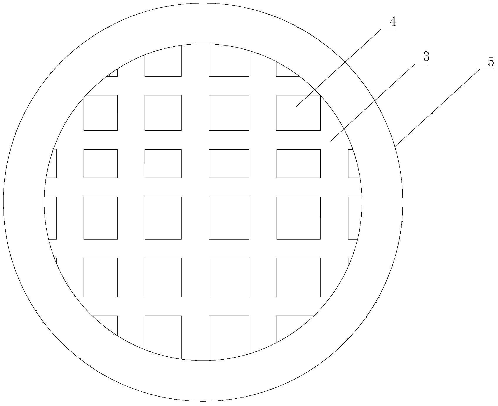
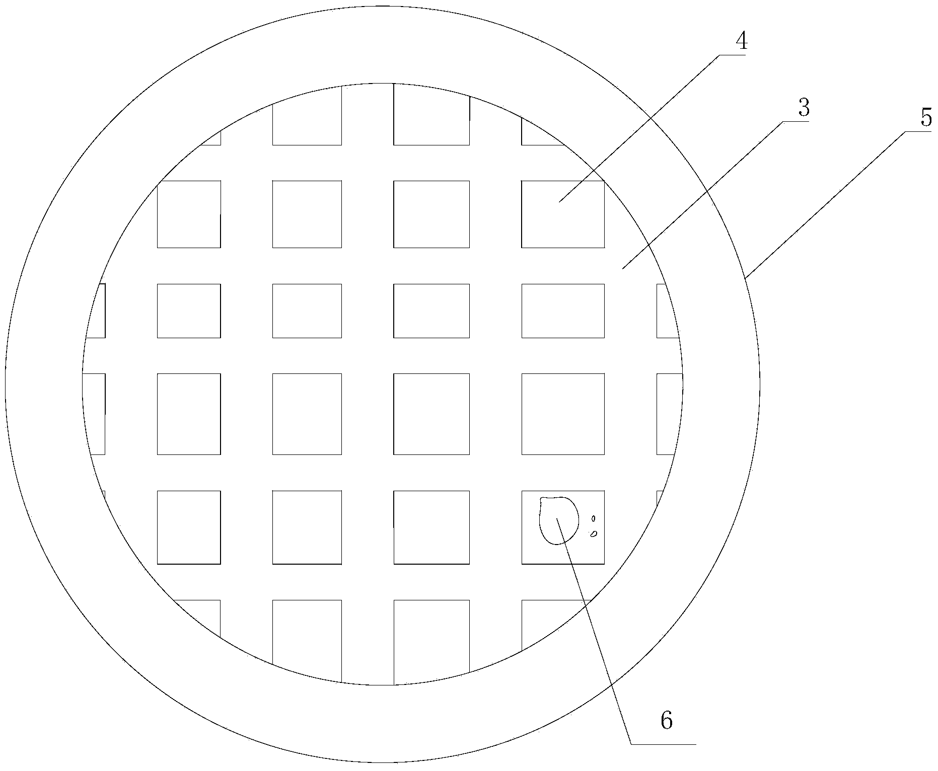
[0033] figure 1 It is a schematic diagram of glass needle adsorption sample of the present invention; as figure 1 As shown, in the semiconductor industry, focused ion beams are mostly used to prepare transmission electron microscope samples, and then a sampling system (not shown in the figure) is used to bring a glass needle 2 with a needle head 10 with a diameter of 0.2-0.5 μm close to the prepared sample 1 , using the electrostatic force between the ...


PUM

PropertyMeasurementUnit
Diameteraaaaaaaaaa

Abstract

The invention provides a method for improving the success rate of a transmission electron microscope's irradiation on a sample. The sample and a damaged carbon film are extracted by the adsorption force of a glass needle in a sampling system, the sample is placed in an intact area on the upper surface of the carbon film, and the transmission electron microscope is employed to photograph the sample again, so that the damage rate of the sample is effectively reduced, the success rate of the transmission electron microscope's irradiation on the sample is improved, and the cost of the process is lowered.

Description

technical field [0001] The invention belongs to the field of transmission electron microscopes, in particular to a method for improving the success rate of irradiation of samples by a transmission electron microscope. Background technique [0002] Transmission Electron Microscope (hereinafter referred to as TEM), which can simultaneously analyze microstructure morphology, crystal structure, constituent elements, chemical bonding state and electron distribution structure, is one of the powerful tools for solid material analysis. [0003] With the continuous development of the semiconductor industry, the continuous improvement of technology, the continuous reduction of chip size, and the increasingly diversified, three-dimensional, and miniaturized growth of materials, the interfaces, strain states, strain relaxation and The subsequent formation of lattice mismatch dislocations, etc., provides a broad development space for the use of TEM. [0004] Since the imaging principle ...

Claims


Application Information

Patent Timeline
IPC IPC(8): G01N23/225
Inventor 高林唐涌耀陈强高金德
Owner SHANGHAI HUALI MICROELECTRONICS CORP
Why Eureka
Try Eureka