Stimulation based detection method for SiGe hetero-junction bipolar transistor (HBT) single event effects

A heterojunction bipolar and single-event effect technology, which is applied in the testing of a single semiconductor device, can solve problems such as the inability to guarantee the beam current time, the difficulty in accurately locating the sensitive position of a device's single-event failure, and the inability to quantitatively analyze the failure mechanism. Achieve the effect of saving test funds and time, ensuring efficiency and accuracy

Inactive Publication Date: 2014-03-19
XINJIANG TECHN INST OF PHYSICS & CHEM CHINESE ACAD OF SCI
View PDF6 Cites 14 Cited by
  • Summary
  • Abstract
  • Description
  • Claims
  • Application Information

AI Technical Summary

Problems solved by technology

The single event effect based on the ground simulation test depends on the limitation of domestic heavy ion sources, and the beam time cannot be guaranteed
At the same time, as the size of the device enters the micron or even deep sub-micron range, it is difficult to realize the micron-level beam current in the evaluation of the single event effect based on the ground simulation experiment, so it is difficult to accurately locate the sensitive position of the single event failure of the device, and it is impossible to quantitatively analyze the mechanism of the failure

Method used


Image

  • Stimulation based detection method for SiGe hetero-junction bipolar transistor (HBT) single event effects
  • Stimulation based detection method for SiGe hetero-junction bipolar transistor (HBT) single event effects
  • Stimulation based detection method for SiGe hetero-junction bipolar transistor (HBT) single event effects

Examples


Embodiment

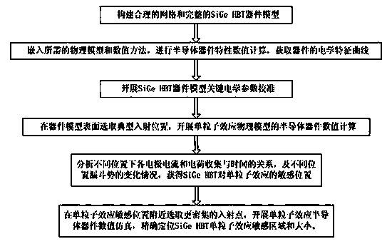
[0046] The present invention provides a single event effect sensitive region detection technology based on three-dimensional device simulation, which realizes the theoretical evaluation of single event effect;

[0047] figure 1 It is a flow chart of SiGe HBT single event effect sensitive area detection technology based on 3D device simulation;

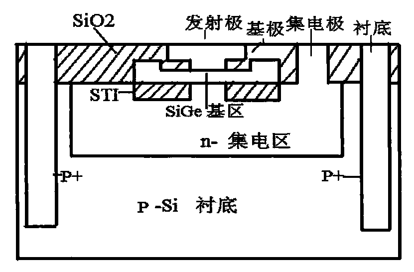
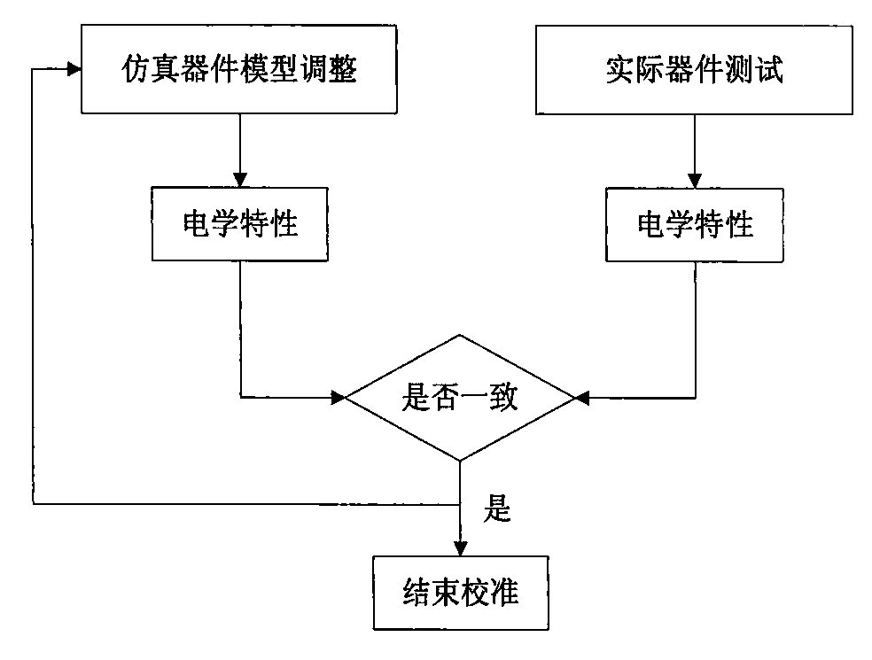
[0048] In step a, use the specific editing language of the 3D simulation software to realize the actual 3D geometric structure, regional material, and doping distribution of the silicon-germanium heterojunction bipolar transistor (SiGe HBT), and construct a reasonable grid and a complete device model. Various parameters are edited into the simulation input file using the software editing language; in order to effectively and accurately simulate the single event effect of the device, it is very important to establish a reasonable grid. A small number of grids will affect the accuracy of the simulation, and too many grids will consume F...


PUM


Abstract

The invention provides a stimulation based detection method for SiGe HBT single event effects. The method comprises establishing a reasonable SiGe HBT device model and network; stimulating semiconductor device characteristics of the established SiGe HBT device model; performing key electrical parameter correction on the SiGe HBT device model; selecting a typical incidence position on the surface of the device model to perform single event effect physical model stimulation; analyzing the relation between current and charge collection of all poles and time at different positions and funnel potential change conditions of different positions to obtain the sensitive position of the SiGe HBT towards the single event effect; selecting denser incidence points nearby the single event effect sensitive position, performing stimulation on single event effect semiconductor device numerical values, and locating HBT single event effect sensitive areas and amplitudes accurately. The method has the advantages that damage of the single event effect is analyzed theoretically and quantitatively, assessment time is shortened, test costs are reduced and the like.

Description

technical field [0001] The invention relates to a single event effect detection method of a semiconductor device, in particular to a single event effect sensitive area positioning technology based on three-dimensional device simulation, belonging to the technical field of microelectronics and the field of anti-radiation reinforcement technology. Background technique [0002] With the continuous development of microelectronics technology, IC technology and computer technology, electronic design automation tools have become an important means of research and development of semiconductor devices. The simulation technology of semiconductor device manufacturing and processing is to establish a corresponding mathematical physical model based on the actual manufacturing process, integrate the simulation analysis of the process and the physical characteristics of the device, replace expensive and time-consuming process experiments, and obtain the ideal device structure. It provides ...

Claims


Application Information

Patent Timeline
Patent Type & Authority Applications(China)
IPC IPC(8): G01R31/26
Inventor 郭红霞郭旗张晋新文林陆妩余学峰何承发崔江维孙静席善斌邓伟王信
Owner XINJIANG TECHN INST OF PHYSICS & CHEM CHINESE ACAD OF SCI
Why Eureka
Try Eureka