Printing type paper microfluid chip and manufacture method thereof

A paper-based microfluidics, manufacturing method technology, applied in chemical instruments and methods, laboratory utensils, laboratory containers, etc. Cost, reduce complexity, and improve production efficiency

Active Publication Date: 2014-03-26
TECHNICAL INST OF PHYSICS & CHEMISTRY - CHINESE ACAD OF SCI
View PDF6 Cites 34 Cited by
  • Summary
  • Abstract
  • Description
  • Claims
  • Application Information

AI Technical Summary

Problems solved by technology

However, the great difficulty faced by paper microfluidic device technology lies in the fabrication of various sensors on its surface. Even devices such as electrodes can only be realized through complex processes such as high-temperature evaporation and electrochemica

Method used


Image

  • Printing type paper microfluid chip and manufacture method thereof
  • Printing type paper microfluid chip and manufacture method thereof
  • Printing type paper microfluid chip and manufacture method thereof

Examples


Embodiment 1

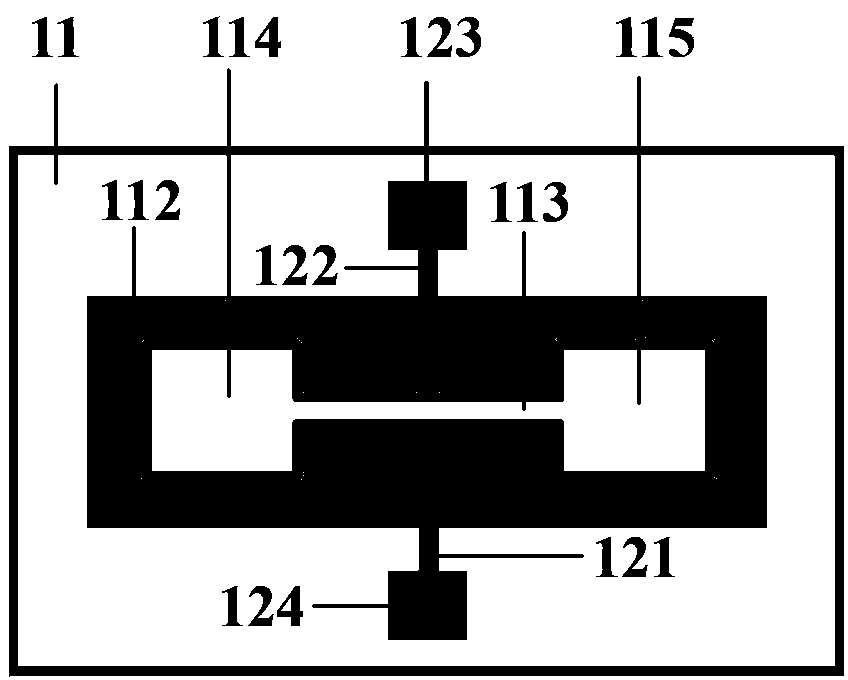
[0036] figure 2It is a schematic structural diagram of a printed paper microfluidic chip in Example 1 of the present invention, as figure 2 As shown, in this embodiment, the microfluidic chip substrate 11 is made of paper with a thickness of 0.5mm, and its part is infiltrated with paraffin to form figure 2 In the rectangular paraffin paper part 112, on this basis, a metal hard mold is used to emboss a flow channel 113 with a width of 0.1 mm on the paraffin paper part 112, and a fluid inlet pool 114 and an outlet pool 115 of 2 mm × 2 mm at both ends of the flow channel After that, at room temperature, the conductive metal ink (liquid gallium) 121 containing 0.25wt% gallium oxide is vertically coated on the upper and lower sides of the flow channel 113 in the paraffin paper 112 in the form of a line, forming an electrode 121 with a width of 0.5mm , 122, where the ends of the two electrodes are terminals 123, 124 of 2mm×2mm. Thus, the fabrication of the flow cytometry chip o...

Embodiment 2

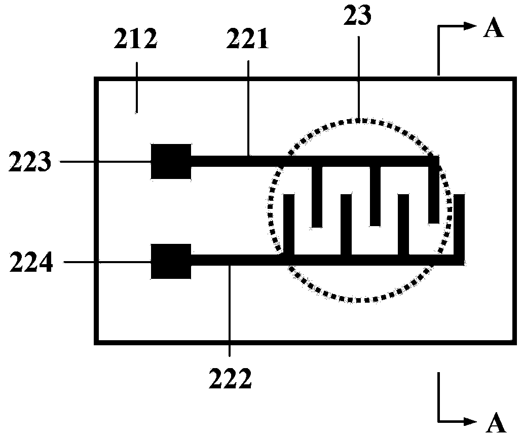
[0038] Figure 3a It is a schematic structural diagram of a printed paper microfluidic chip in Example 2 of the present invention, Figure 3b for Figure 3a A-A sectional view, such as Figure 3a-3b As shown in Fig. 1, the liquid drop directly titrated on the substrate is measured by using a channelless structure, and the electrode shape adopts a toothed structure to improve sensitivity. In this embodiment, the microfluidic chip substrate 212 is made of paper with a thickness of 0.5mm, which is completely infiltrated with paraffin; after that, at room temperature, the conductive metal ink (liquid gallium) containing 0.25wt% gallium oxide is coated in a tooth-shaped staggered form. Cover the surface of paraffin paper to form tooth-shaped electrodes 221 and 222 with a line width of 0.5 mm, and the ends of the two electrodes are terminals 223 and 224 of 2 mm×2 mm. Thus, the fabrication of the droplet fluid detection chip of this embodiment is completed. When in use, once the ...

Embodiment 3

[0040] Figure 4 It is a schematic structural diagram of a printed paper microfluidic chip in Example 3 of the present invention, as Figure 4 As shown, the difference between Embodiment 1 and Embodiment 2 is that the function of the electrode here is to exist as a heating film. In this embodiment, the microfluidic chip substrate 31 uses paper with a thickness of 0.5 mm, and its part is infiltrated with paraffin. On this basis, a metal hard mold is used to imprint a width of 0.1 mm on the paraffin paper part in a meandering form as shown in the figure. The flow channel 312 of mm, the two ends of the flow channel are a fluid inlet pool 313 and an outlet pool 314 of 2mm×2mm; after that, a metal ink (liquid gallium) 321 containing 0.25wt% gallium oxide is applied in the form of a thin film at room temperature Cover the corresponding parts of the paraffin paper, thereby forming three-stage heating films 33, 34, 35 with a width of 5mm, respectively, and the respective heating powe...


PUM

PropertyMeasurementUnit
Particle sizeaaaaaaaaaa

Abstract

The invention discloses a printing type paper microfluid chip and a manufacture method thereof. The chip comprises one or an integrated component of a paper base, an electrode formed by conductive metal ink, a heater, a thermosensitive sensor, a photosensitive sensor, a magneto-dependent sensor, a piezoelectric sensor, a humidity-dependent sensor, an electrochemical sensor and an electrode array electric wetting pump. The printing type paper microfluid chip and the manufacture method thereof provided by the invention have the advantages that a low-melting-point liquid metal ink is introduced, sensor pieces arranged on the whole chip can be directly manufactured in a printing manner, so that the chip is obtained; the chip is finished in a preparation process under the normal temperature and normal condition, the common biodegradability paper is adopted as a base, the environmental requirement is not high, the complexity of the preparation technology of the microfluid chip is remarkably reduced, the manufacture efficiency is greatly improved, and the cost is reduced.

Description

technical field [0001] The invention relates to the technical field of microfluidic chips, in particular to a printed paper microfluidic chip and a manufacturing method thereof. Background technique [0002] Micro / nanofluidic devices are an important branch of MEMS. Because it has the characteristics of small size, small invalid volume, low power consumption, high control precision, fast response speed, etc., and it is easy to batch process and realize the integration of fluid devices and control circuits such as micro pumps, micro valves, micro flow sensors, etc., so in There are increasingly widespread applications in many fields. In the past few decades, with the wide application of microfluidic systems in disease detection, biochemical analysis, DNA sequencing, drug screening and delivery, in vivo environment detection and other biotechnology, the miniaturization of sample analysis and detection process has become a One of the most important research areas in systems t...

Claims


Application Information

Patent Timeline
IPC IPC(8): B01L3/00
Inventor 刘静
Owner TECHNICAL INST OF PHYSICS & CHEMISTRY - CHINESE ACAD OF SCI
Why Eureka
Try Eureka