Microelectronic component and corresponding production process

A technology of microelectronics and micromechanical components, which is applied in the directions of microelectronic microstructure devices, electrical components, microstructure technology, etc., can solve the problems of unreliable surface state of sensor elements, and achieve the effect of low cost

Inactive Publication Date: 2014-03-26
ROBERT BOSCH GMBH
View PDF9 Cites 4 Cited by
  • Summary
  • Abstract
  • Description
  • Claims
  • Application Information

AI Technical Summary

Problems solved by technology

The result is surface states that interfere with the field-effect transistor's operating area or cause drift and noise and make the sensor element unreliable

Method used


Image

  • Microelectronic component and corresponding production process
  • Microelectronic component and corresponding production process
  • Microelectronic component and corresponding production process

Examples


Embodiment Construction

[0031] The same reference numbers in the figures indicate identical or functionally identical elements.

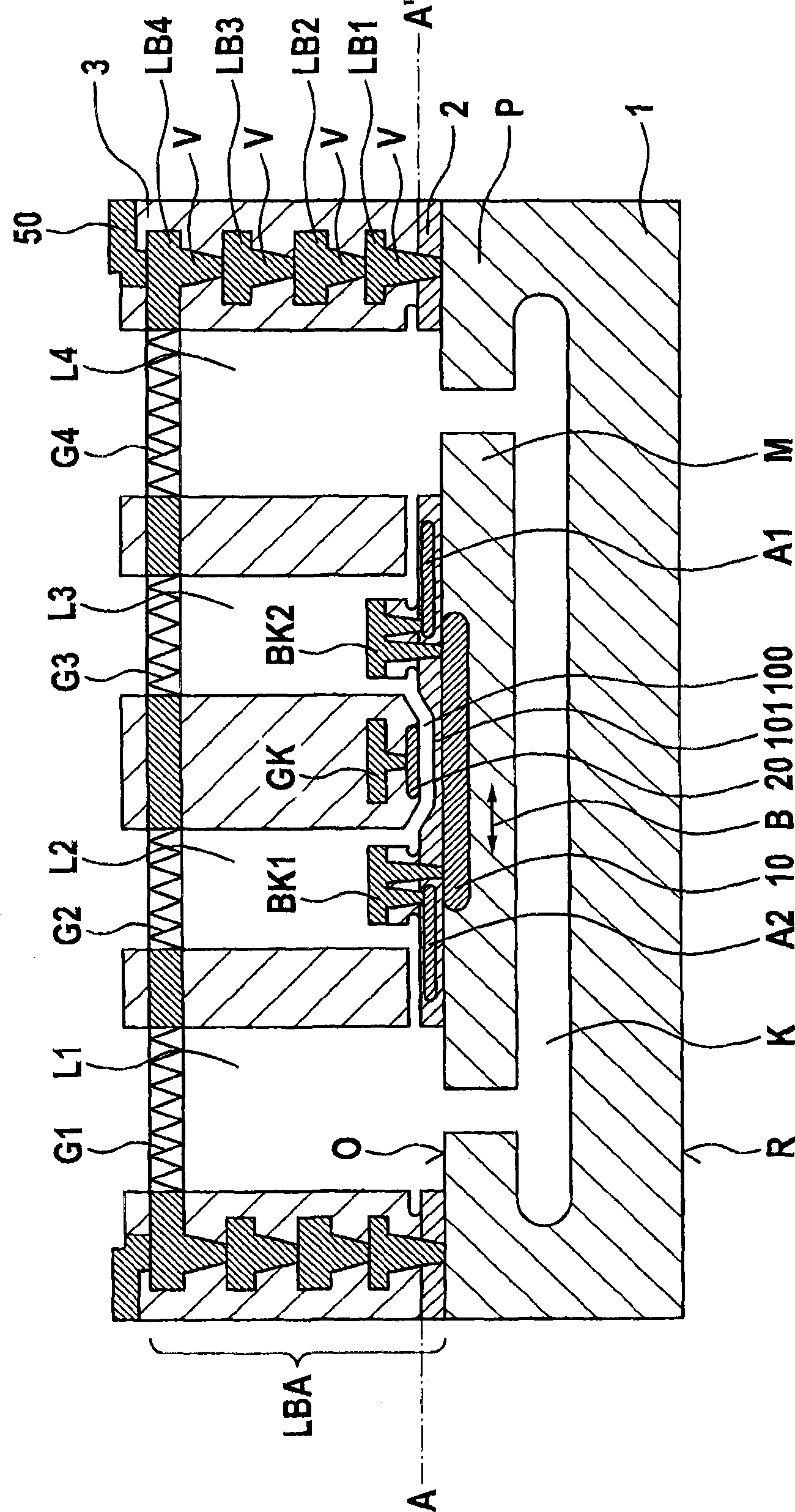
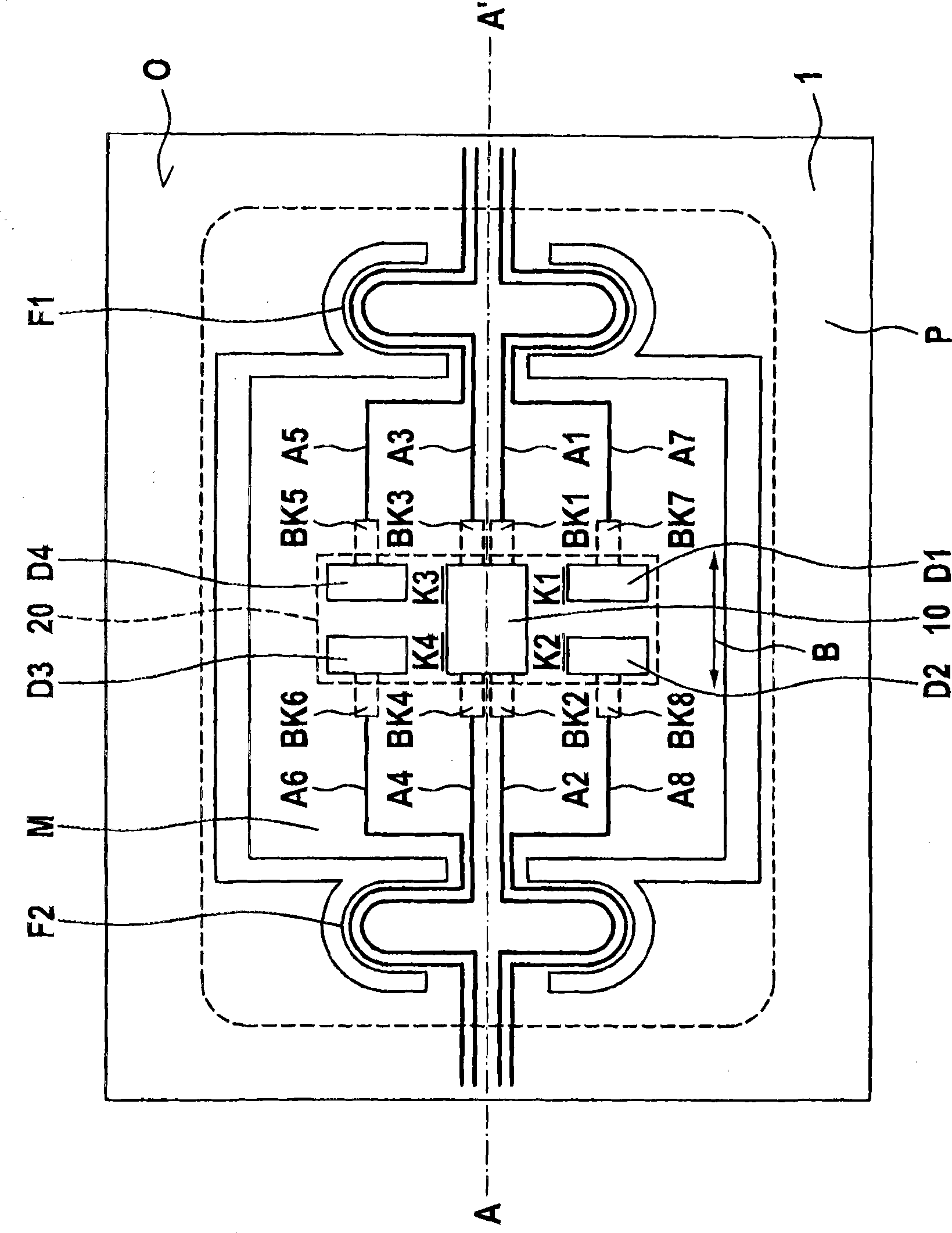
[0032] Figure 1a ), b) are schematic cross-sectional views for illustrating a microelectronic component according to a first embodiment of the present invention, more precisely, Figure 1a ) is the vertical cross-section, while Figure 1b ) is along Figure 1a ) The horizontal cross-section of line A-A'.

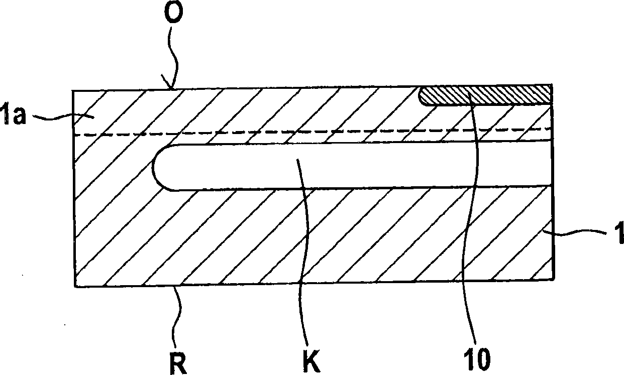
[0033] exist Figure 1a ), b) shows a micromechanical component, which is an inertial sensor with a movable channel. At this time, reference numeral 1 denotes a single-crystal silicon semiconductor substrate having a front surface O and a rear surface R. As shown in FIG.

[0034] The silicon semiconductor substrate 1 has a cavity K on which an elastically deflectable mass device M is arranged, which is connected to the periphery P of the silicon semiconductor substrate 1 via a spring device F1, F2, wherein The spring arrangement consists of a first silicon spring F1 a...


PUM


Abstract

The invention provides a microelectronic component and a corresponding production process. The microelectronic component includes a semiconductor substrate (1;1a) having a top side (O) and a reverse side (R), an elastically movable mass device (M) on the top side (O) of the substrate (1), at least one source region (10;10') provided in or on the mass device (M), at least one drain region (D1-D4;D1'-D10') provided in or on the mass device (M), and a gate region (20;20') suspended on a conductor track arrangement above the at least one source region (10,10' )and at least one drain region (D1-D4;D1'D10') and spaced apart from the mass device by a gap (100). The conductor track arrangement (LBA) is anchored on the top side (O) of the substrate (1) in a periphery (P) of the mass device (M) such that the gate region (20;20') remains fixed when the mass device (M) has been moved.

Description

technical field [0001] The invention relates to microelectronic components and corresponding manufacturing methods. Background technique [0002] Micromechanical sensors, such as inertial sensors, are mainly implemented with the aid of capacitive or piezoresistive transducers. So-called moving grid inertial sensors have been reported in the literature for a long time, however no sensors of this type have been found on the market to date. One reason lies in the type of manufacture of such conversion elements, in particular the preparation of suitable sacrificial layer processes and the availability of CMOS layers with suitable mechanically or thermomechanically well-defined properties. [0003] Silicon oxide is often used as a sacrificial layer in micromechanics. However, in moving gate inertial sensors, the channel region and source / drain contacts are open and unprotected because the thin gate oxide is also forcibly removed when the sacrificial layer is removed. The layer...

Claims


Application Information

Patent Timeline
Patent Type & Authority Applications(China)
IPC IPC(8): B81C1/00B81B7/00B81B3/00
CPCB81B2201/025B81C1/00182G01P15/124B81B7/00B81C1/00G01P15/08H01L29/84H01L29/66477
Inventor C·舍林A·法伊
Owner ROBERT BOSCH GMBH
Why Eureka
Try Eureka