A photonic crystal filter for miniature thermo-optical systems
A photonic crystal and filter technology, applied in the field of spectrum control, can solve the problem that the reflection band of the filter is not wide enough
- Summary
- Abstract
- Description
- Claims
- Application Information
AI Technical Summary
Problems solved by technology
Method used
Image
Examples
Embodiment Construction
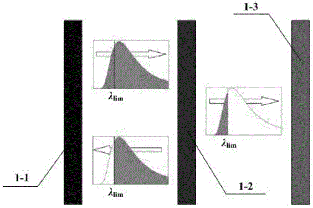
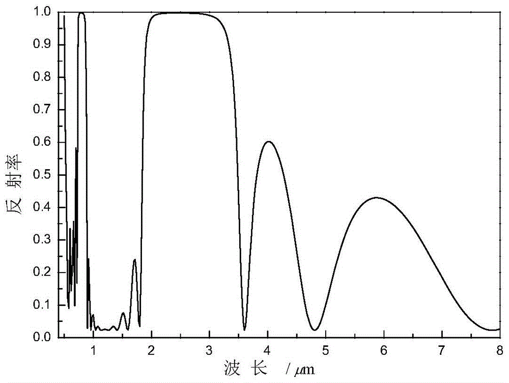
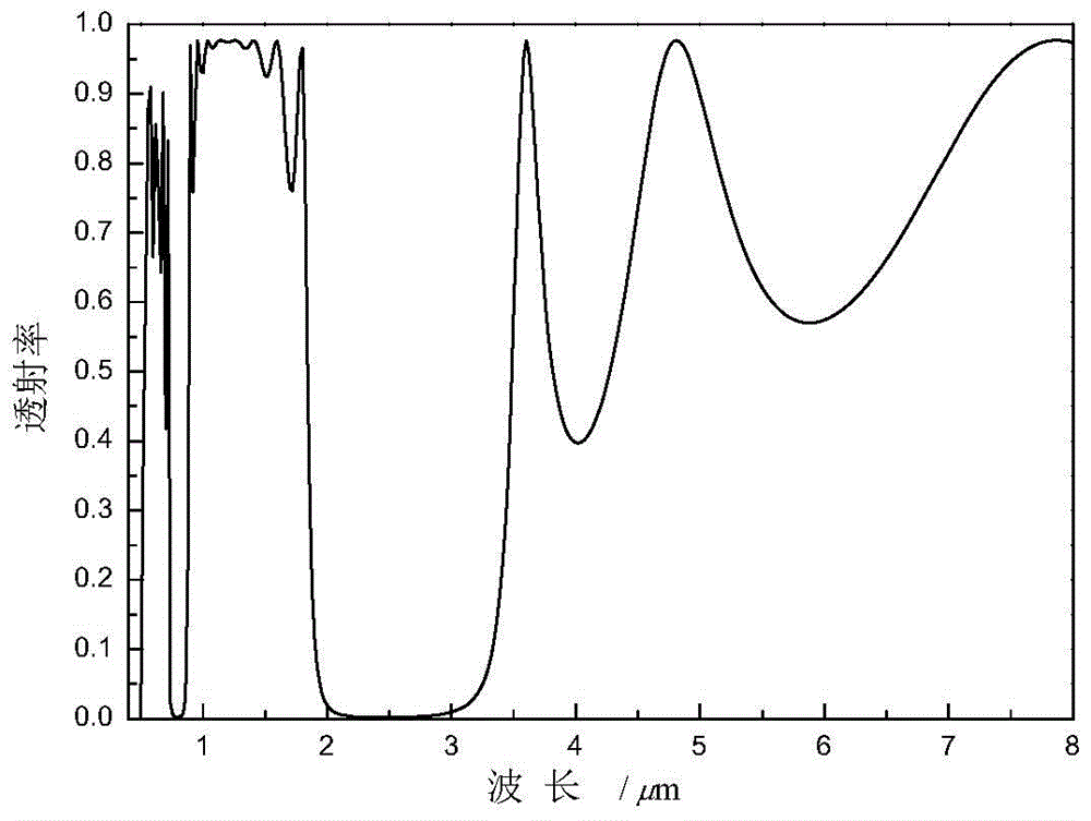
[0024] The specific implementation manner of the present invention will be further described below in conjunction with accompanying drawings 2-5.
[0025] Such as image 3 As shown, the described one-dimensional Si / SiO 2 Photonic crystal filter, composed of two Si / SiO with the center wavelengths of the primary band gap of 2.34 μm and 3.0 μm respectively 2 It is composed of multi-layer superimposed thin films, and the basic structure of the two multi-layer films is (L / 2HL / 2) 5 , after correction and optimization, superimpose them, and the final structure is [1.10(L / 2HL / 2)](L / 2HL / 2)3[1.10(L / 2HL / 2)][0.95(L / 2HL / 2) ](L / 2HL / 2) 3 [0.95(L / 2HL / 2)]. The photonic crystal filter with a new structure has a total of 10 units. Considering that the connected layers between different units are actually the same material, the actual filter has a total of 21 layers, of which 3-1, 3-3, 3-5, 3-7 , 3-9, 3-11, 3-13, 3-15, 3-17, 3-19, 3-21 are SiO 2 Layers, 3-2, 3-4, 3-6, 3-8, 3-10, 3-12, 3-14,...
PUM
 Abstract
Description
Claims
Application Information


