Insulated gate bipolar transistor and preparation method thereof
A technology of bipolar transistors and insulated gates, which is applied in the direction of transistors, semiconductor/solid-state device manufacturing, semiconductor devices, etc., can solve the problems of increasing the difficulty of device manufacturing and small on-state voltage drop, so as to improve the range of high-frequency applications and reduce Effect of on-resistance
- Summary
- Abstract
- Description
- Claims
- Application Information
AI Technical Summary
Problems solved by technology
Method used
Image
Examples
Embodiment 1
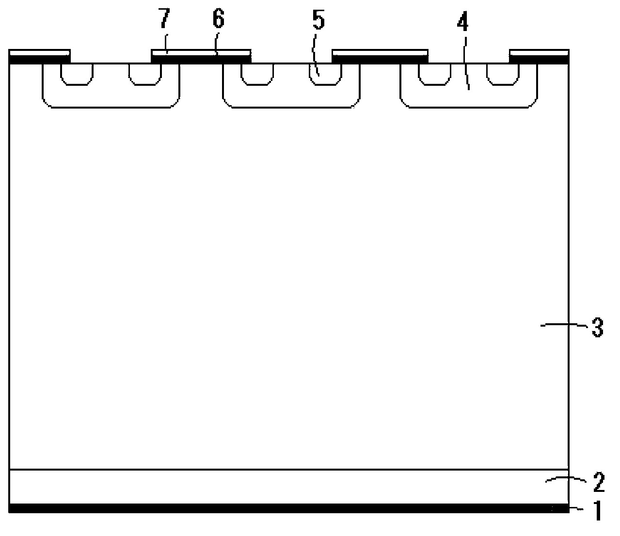
[0012] figure 1 It is a cross-sectional view of an insulated gate bipolar transistor of the present invention, combined below figure 1 The semiconductor device of the present invention will be described in detail.
[0013] An insulated gate bipolar transistor, comprising: a rear P+ emitter region 1, which is a polycrystalline semiconductor silicon material of P conductivity type, with a thickness of 0.2um and a surface doping concentration of boron atoms of 5E17cm -3 ; N+ buffer layer 2, located on the back P+ emitter region 1, is a semiconductor silicon material of N conductivity type, and the doping concentration of phosphorus atoms is 5E13cm -3 ~1E16cm -3 , with a thickness of 30um; the N-base region 3, located on the N+ buffer layer 2, is a semiconductor silicon material of N conductivity type, with a thickness of 200um and a doping concentration of phosphorus atoms of 5E13cm -3 ; P-type base region 4, located on the N-base region 3, is a semiconductor silicon material ...
Embodiment 2
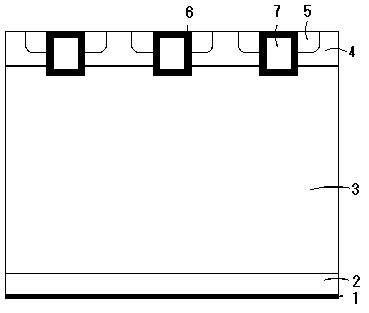
[0021] figure 2 It is a cross-sectional view of the second insulated gate bipolar transistor of the present invention, combined below figure 2 The semiconductor device of the present invention will be described in detail.
[0022] An insulated gate bipolar transistor, comprising: a rear P+ emitter region 1, which is a polycrystalline semiconductor silicon material of P conductivity type, with a thickness of 0.2um and a surface doping concentration of boron atoms of 5E17cm -3 ; N+ buffer layer 2, located on the back P+ emitter region 1, is a semiconductor silicon material of N conductivity type, and the doping concentration of phosphorus atoms is 5E13cm -3 ~1E16cm -3 , with a thickness of 30um; the N-base region 3, located on the N+ buffer layer 2, is a semiconductor silicon material of N conductivity type, with a thickness of 200um and a doping concentration of phosphorus atoms of 5E13cm -3 ; P-type base region 4, located on the N-base region 3, is a semiconductor silicon...
PUM
| Property | Measurement | Unit |
|---|---|---|
| Thickness | aaaaa | aaaaa |
| Thickness | aaaaa | aaaaa |
| Doping concentration | aaaaa | aaaaa |
Abstract
Description
Claims
Application Information
 - R&D
- Intellectual Property
- Life Sciences
- Materials
- Tech Scout
- Unparalleled Data Quality
- Higher Quality Content
- 60% Fewer Hallucinations
Browse by: Latest US Patents, China's latest patents, Technical Efficacy Thesaurus, Application Domain, Technology Topic, Popular Technical Reports.
© 2025 PatSnap. All rights reserved.Legal|Privacy policy|Modern Slavery Act Transparency Statement|Sitemap|About US| Contact US: help@patsnap.com


