High thermal conductivity metal substrate and manufacturing method thereof

A technology of metal substrate and manufacturing method, which is applied in the directions of printed circuit manufacturing, printed circuit components, electrical components, etc. features, etc.

Active Publication Date: 2014-04-02
江苏生益特种材料有限公司
View PDF18 Cites 10 Cited by
  • Summary
  • Abstract
  • Description
  • Claims
  • Application Information

AI Technical Summary

Problems solved by technology

[0007] At present, the application of LCP in copper clad laminates mainly focuses on the production of copper clad laminates for high frequency circuits. Although this kind of board has excellent dielectric properties, the thermal conductivity of the whole board is not good...

Method used


Image

  • High thermal conductivity metal substrate and manufacturing method thereof
  • High thermal conductivity metal substrate and manufacturing method thereof
  • High thermal conductivity metal substrate and manufacturing method thereof

Examples


Embodiment 1

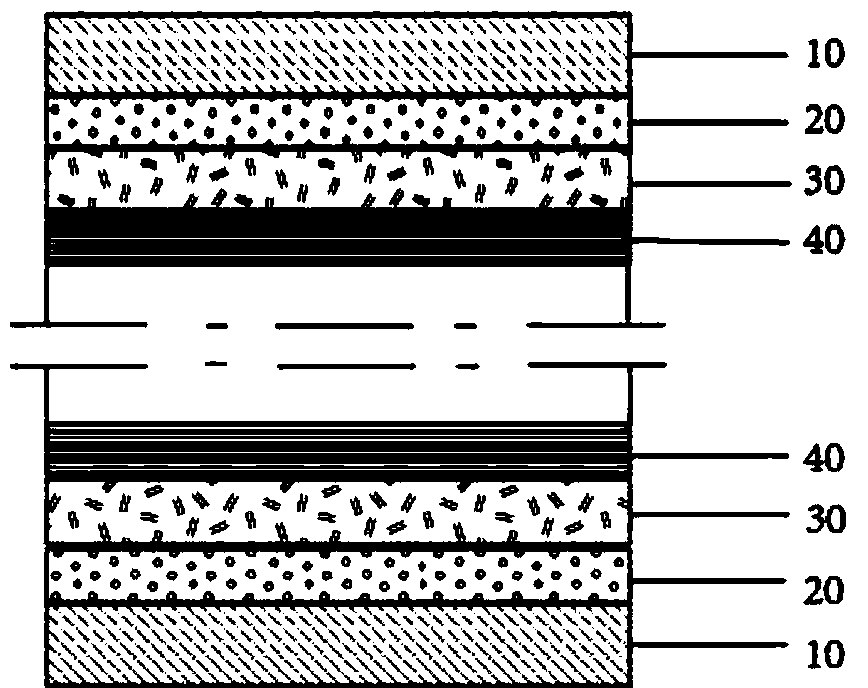
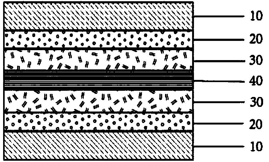
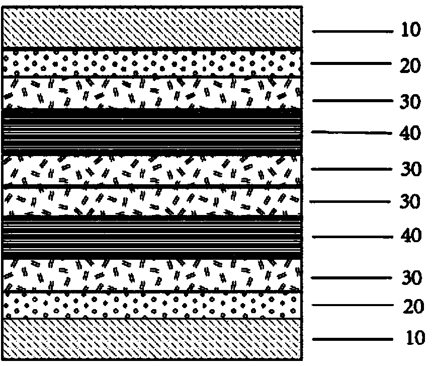
[0074] On each side of a porous LCP film with a thickness of 50μm and a porosity of 50%, a 15μm thick cyanate ester thermal conductive glue with a thermal conductivity of 4.0W / mK is coated on each side. After heating and baking, the LCP is reinforced The prepreg of the material: Coat a layer of 40μm thick epoxy thermal conductive glue with a thermal conductivity of 2.0W / mK on the roughened surface of the 35μm copper foil. After heating and baking, the glued copper foil is obtained, according to the glued copper foil / LCP prepreg / coated copper foil laminated structure for lamination, the specific structure is as figure 2 , The above-mentioned prepared laminated blank material is sandwiched between two mirror stainless steel plates, and then put into the laminator, at a temperature of 200℃, a pressure of 4MPa, and a pressing time of 90 minutes to obtain a high thermal conductivity metal substrate .

Embodiment 2

[0076] Coat each side of a porous LCP film with a thickness of 50μm and a porosity of 70% with a thickness of 15μm with the above-mentioned cyanate ester thermal conductive glue with a thermal conductivity of 4.0W / mK. After heating and baking, the LCP is reinforced The prepreg of the material: Coat a layer of 40μm thick epoxy thermal conductive glue with a thermal conductivity of 2.0W / mK on the roughened surface of the 35μm copper foil. After heating and baking, the glued copper foil is obtained, according to the glued copper foil / LCP prepreg / coated copper foil laminated structure for lamination, the specific structure is as figure 2 , The above-mentioned prepared laminated blank material is sandwiched between two mirror stainless steel plates, and then put into the laminator, at a temperature of 200℃, a pressure of 4MPa, and a pressing time of 90 minutes to obtain a high thermal conductivity metal substrate .

Embodiment 3

[0078] Coat each side of the porous LCP film with a thickness of 50μm and porosity of 90% with a thickness of 15μm with the above-mentioned cyanate ester thermal conductive glue with a thermal conductivity of 4.0W / mK. After heating and baking, the LCP is reinforced The prepreg of the material: Coat a layer of 40μm thick epoxy thermal conductive glue with a thermal conductivity of 2.0W / mK on the roughened surface of the 35μm copper foil. After heating and baking, the glued copper foil is obtained, according to the glued copper foil / LCP prepreg / coated copper foil laminated structure for lamination, the specific structure is as figure 2 , The above-mentioned prepared laminated blank material is sandwiched between two mirror stainless steel plates, and then put into the laminator, at a temperature of 200℃, a pressure of 4MPa, and a pressing time of 90 minutes to obtain a high thermal conductivity metal substrate .


PUM

PropertyMeasurementUnit
Thermal conductivityaaaaaaaaaa
Thicknessaaaaaaaaaa

Abstract

The invention relates to a high thermal conductivity metal substrate and a manufacturing method thereof. The high thermal conductivity metal substrate comprises a porous liquid crystal polymer (LCP) film, heat conducting insulation layers which are coated on two sides of the porous LCP film and have the thermal conductivity of 2-6W/m.K, a heat conducting insulation layer which is coated on a metal foil and has the thermal conductivity of 1-4W/m.K, and the metal foil. The two sides of the porous LCP film and one side of the metal foil are coated with the heat conducting insulation layers, and the high thermal conductivity metal substrate is prepared through lamination. The prepared metal substrate has high thermal conductivity and excellent dielectric properties.

Description

Technical field [0001] The invention relates to a metal substrate and a manufacturing method thereof, in particular to a high thermal conductivity metal substrate for high-frequency circuits and a manufacturing method thereof. Background technique [0002] In recent years, with the development of high-performance and high-functionality of computers and information communication equipment, in order to be able to transmit and process large-capacity information at a high speed, the operation signal has become more and more high-frequency, so higher requirements have been proposed for electronic circuit substrates. Among the requirements, this includes excellent dielectric properties, that is, low dielectric constant and low dielectric loss factor. Moreover, the "lighter, thinner, shorter, and smaller" electronic products have made the integration of circuit boards higher and higher, more and more components are mounted, and more and more heat per unit area is emitted during work. E...

Claims


Application Information

Patent Timeline
IPC IPC(8): H05K1/02H05K3/00
Inventor 邓华阳许永静黄增彪
Owner 江苏生益特种材料有限公司
Why Eureka
Try Eureka