Novel GaN-based LED structure and manufacturing method thereof

An LED structure, p-type technology, applied in electrical components, circuits, semiconductor devices, etc., can solve the problems of low luminous efficiency and high operating voltage of GaN-based LEDs, and achieve the effect of avoiding damage and improving crystal quality.

Active Publication Date: 2014-04-09
SUZHOU JUZHEN PHOTOELECTRIC
View PDF5 Cites 13 Cited by
  • Summary
  • Abstract
  • Description
  • Claims
  • Application Information

AI Technical Summary

Problems solved by technology

[0005] For this reason, the technical problem to be solved by the present invention lies in the problems of low luminous efficiency and high working voltage of GaN-based LEDs in the prior art, thereby proposing a new structure and preparation method of GaN-based LEDs

Method used


Image

  • Novel GaN-based LED structure and manufacturing method thereof
  • Novel GaN-based LED structure and manufacturing method thereof
  • Novel GaN-based LED structure and manufacturing method thereof

Examples


Embodiment Construction

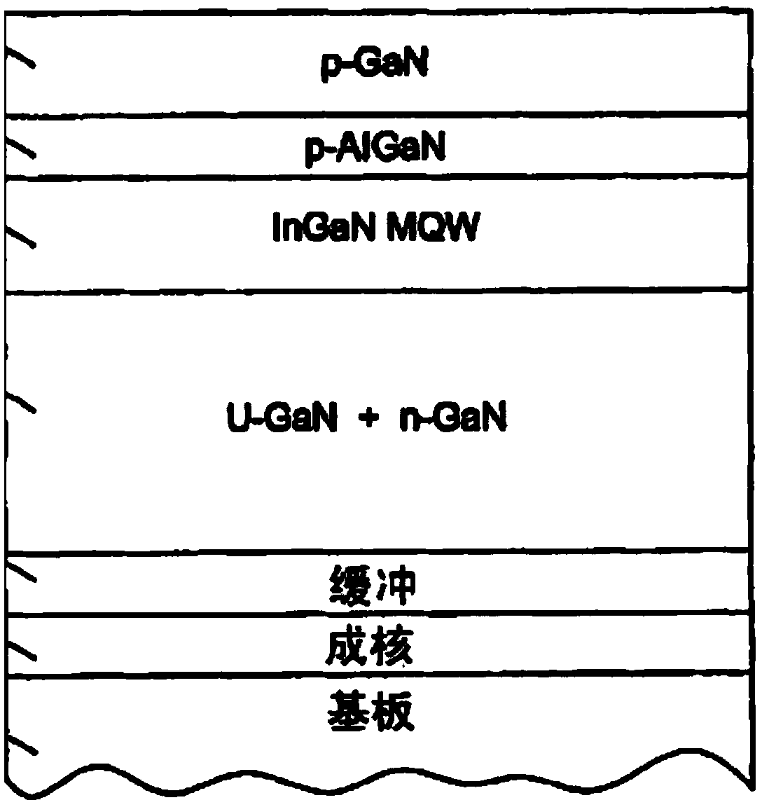
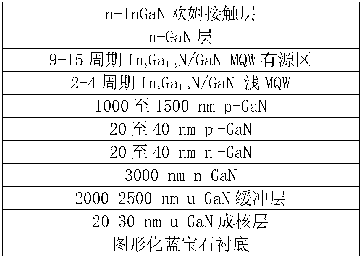
[0032] According to one embodiment of the present invention, figure 2 It is the new GaN-based LED structure described in the present invention, which includes from bottom to top: patterned sapphire substrate, 20-30nm undoped GaN buffer layer, 2000-2500nm undoped GaN buffer layer, 3000nm doped Si n-type GaN, 20 to 40nm highly doped Si n + type GaN, 20 to 40nm highly doped Mg p + Type GaN, 1000 to 1500nm Mg-doped p-type GaN, 2-4 period In x Ga 1-x N / GaN shallow MQW, In y Ga 1-y N / GaN MQW active region quantum well layer (where y is greater than x), GaN barrier layer, Si-doped n-type GaN layer, and Si-doped InGaN ohmic contact layer.

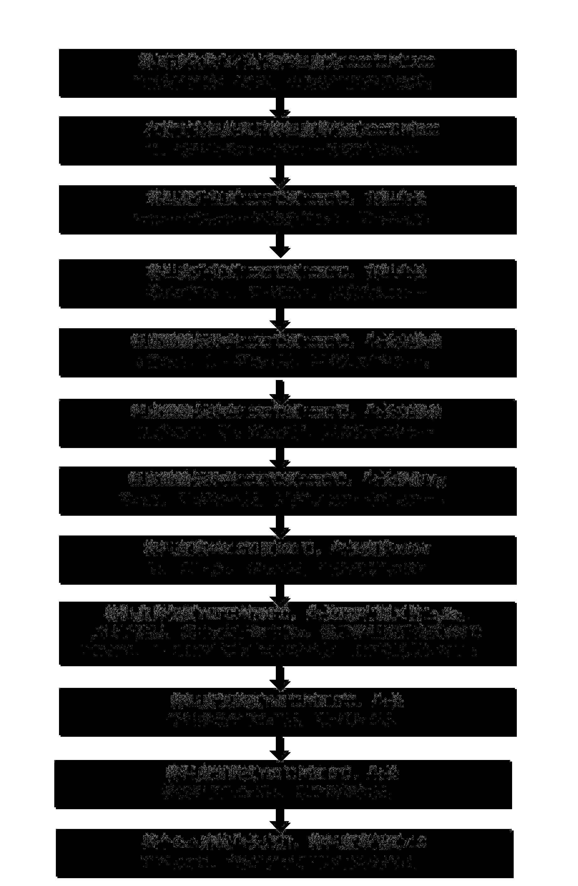
[0033] According to one embodiment of the present invention, image 3 For the specific growth process of the GaN-based LED structure, the main treatment plan is to grow p-type GaN first, then grow the intermediate multi-layer quantum well structure (MQW), and then grow the n-type GaN layer. The specific structure growth process is described as...


PUM


Abstract

The invention provides a novel GaN-based LED structure and a manufacturing method of the novel GaN-based LED structure, and belongs to the field of semiconductor photoelectronic device manufacturing. Compared with the prior art, the novel GaN-based LED structure and the manufacturing method of the novel GaN-based LED structure are characterized in that a p- type GaN epitaxial layer doped with Mg grows on a p+ -GaN layer and an n+ -GaN layer at a high temperature; Si atoms in the n+ -GaN layer can effectively restrain forming of point defects and the luminescence quenching phenomenon of the GaN epitaxial layer, and the p+ -GaN layer is beneficial for improving hole current injection efficiency and reducing the working voltage of an LED; because the GaN-based LED grows on the p+ -GaN layer and the n+ -GaN layer at the high temperature, the crystalline quality, the hole concentration and the mobility ratio of the p- type GaN are improved, and accordingly the efficiency of injecting hole current into a quantum well active area and the luminous efficiency of the LED are improved.

Description

technical field [0001] The invention relates to a novel GaN-based LED structure and a preparation method, belonging to the field of preparation of semiconductor optoelectronic devices. Background technique [0002] Gallium nitride (GaN)-based light-emitting diodes (LEDs) have been widely used in many fields such as full-color display and solid-state lighting, which all depend on the growth of Mg-doped p-type GaN to achieve high-brightness blue and green light. The production of light LED has become a reality, and its position in commercial applications is becoming more and more important. The initial basic structure of the LED is a homogeneous PN junction. In order to improve the efficiency of light emission, a multi-layer quantum well structure, namely multiple quantum well (MQW), is added in the middle of the PN junction. The current LED structure growth is to first grow n-type GaN, then grow the middle quantum well (MQW) structure, and then grow the p-type GaN layer, tha...

Claims


Application Information

Patent Timeline
Patent Type & Authority Applications(China)
IPC IPC(8): H01L33/20H01L33/22
CPCH01L33/0075H01L33/325
Inventor 杨晓杰李晓东
Owner SUZHOU JUZHEN PHOTOELECTRIC
Why Eureka
Try Eureka