Thin film transistor

A thin film transistor and semiconductor technology, applied in transistors, semiconductor devices, electrical components, etc., can solve the problems of increasing pixel circuit area, large parasitic resistance, increasing the complexity of driving circuits, etc., to reduce threshold voltage drift, reduce device degradation, The effect of improving reliability

Active Publication Date: 2014-04-16
SUZHOU UNIV
View PDF4 Cites 7 Cited by
  • Summary
  • Abstract
  • Description
  • Claims
  • Application Information

AI Technical Summary

Problems solved by technology

However, the LDD structure will increase the process difficulty of the TFT device, and will introduce a large parasitic resistance, thereby affecting the on-state characteristics of the device
[0004] At present, in AMOLED pixel circuits, threshold voltage compensation is generally based on circuit design technology to cope with performance drift caused by TFT devices under long-term operation, which greatly increases the complexity of the driving circuit and increases the area of ​​the pixel circuit.

Method used


Image

  • Thin film transistor
  • Thin film transistor
  • Thin film transistor

Examples


Embodiment 1

[0043] ginseng Figure 4a , 4b As shown, the thin film transistor device structure in this embodiment is a top-gate self-aligned structure, including: an insulating substrate 100, a source-drain region 101, a semiconductor channel region 102, a gate insulating layer 103, a gate 104, and a passivation layer 105 , the source and drain electrodes 106 and the carrier injection region 107 .

[0044] The carrier injection region 107 is in the same layer as the semiconductor channel region 102, and is located on both sides of the semiconductor channel region 102 and is in close contact with the semiconductor channel region 102. The carrier injection region 107 is used to provide the semiconductor channel region 102 with a carrier. Ryuko.

Embodiment 2

[0046] ginseng Figure 5a , 5b As shown, the TFT device structure in this embodiment is a top-gate self-aligned structure, including: an insulating substrate 200, a source-drain region 201, a semiconductor channel region 202, a gate insulating layer 203, a gate 204, and a passivation layer 205 , source and drain electrodes 206 and carrier injection layer 207 .

[0047] The carrier injection layer 207 is located below the semiconductor channel region 202 and is in close contact with the semiconductor channel region 202 , and can provide carriers to the semiconductor channel region 202 .

Embodiment 3

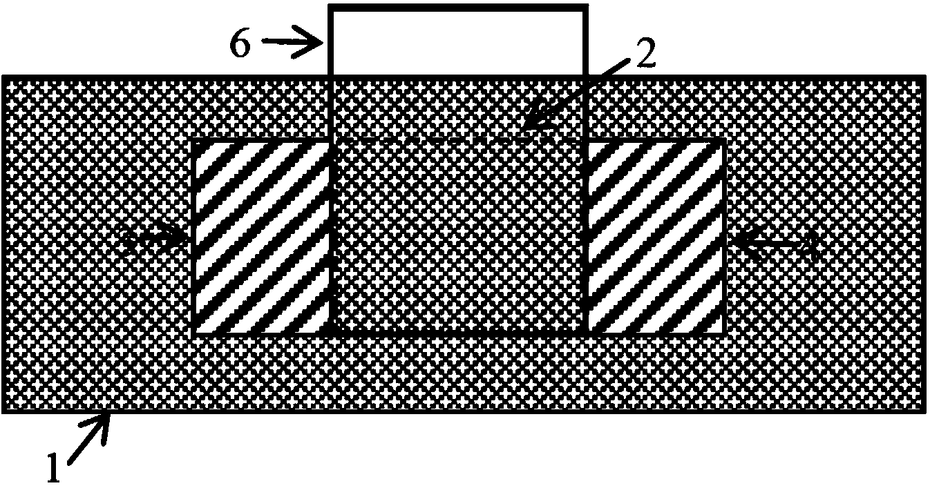
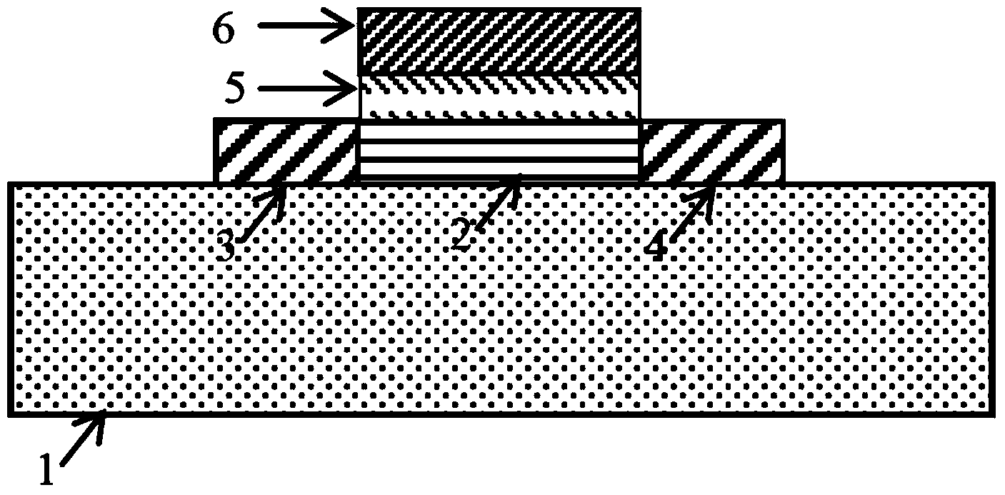
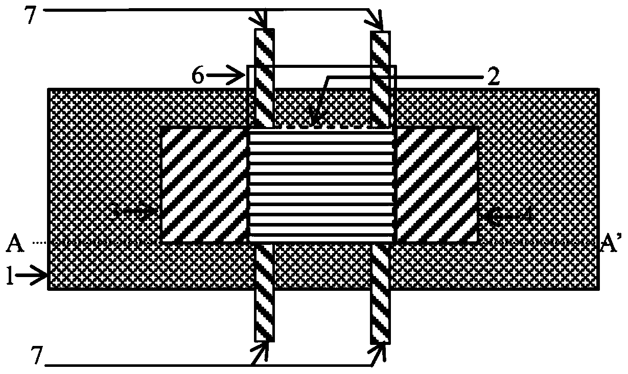
[0049] ginseng Figure 6a , 6b As shown, the TFT device structure in this embodiment is a bottom-gate structure, including: an insulating substrate 300 , a gate 301 , a gate insulating layer 302 , a semiconductor channel region 303 , source and drain electrodes 304 and a carrier injection layer 305 .

[0050] The carrier injection layer 305 is above the semiconductor channel region 303 and in close contact with the semiconductor channel region 303 . Carriers can be provided by the carrier injection layer 305 , and provide carriers to the channel through the region where the carrier injection layer 305 is in contact with the semiconductor channel region 303 .

[0051] In this embodiment, it can be as Figure 6a As shown, the carrier injection layer 305 is designed in segments, and the middle position of the semiconductor channel region 303 is not provided with a carrier injection layer. Of course, in other implementation modes, such as Figure 6c As shown, the carrier inject...


PUM


Abstract

The invention discloses a thin film transistor. The thin film transistor comprises a substrate, a semiconductor channel region, a gate insulating layer, a source region, a leakage region, a source electrode, a leakage electrode and a gate electrode. The thin film transistor further comprises a current carrier injection structure. The thin film transistor can remarkably reduce device degradation and threshold voltage drift, the device and circuit reliability of the thin film transistor is improved, the complexity of the threshold voltage compensating circuit design is simplified. In addition, the thin film transistor is low in process difficulty and does not influence normal work of devices.

Description

technical field [0001] The present invention relates to the technical field of semiconductors, in particular to a thin film transistor (Thin Film Transistor, TFT) that realizes the injection structure of different types of carriers and improves device reliability. Background technique [0002] The active-driven AMOLED (Active matrix Organic Light-Emitting Diode) display technology that combines TFT devices with OLED (Organic Light-Emitting Diode) technology is an important development direction for current and future flat panel displays. For (but not limited to) such applications, the reliability of TFT devices is a device performance that is generally concerned in the industry. [0003] In the DC working state of the transistor device, the high voltage will generate a high electric field near the drain terminal, which will cause the hot carrier effect and cause the degradation of the device performance. In order to reduce the hot carrier effect, it can be solved by reducin...

Claims


Application Information

Patent Timeline
Patent Type & Authority Applications(China)
IPC IPC(8): H01L29/786
CPCH01L29/78618H01L29/45H01L29/7839H01L29/78612H01L29/78696H01L29/0607
Inventor 王明湘王槐生张冬利
Owner SUZHOU UNIV
Why Eureka
Try Eureka