Touch circuit, touch circuit unit, touch display panel and touch display device

A touch circuit and touch technology, which is applied in the input/output process of electrical digital data processing, instruments, data processing, etc. Action and other issues, to achieve the effect of simple structure, sensitive response and high integration

Active Publication Date: 2014-04-30
PEKING UNIV SHENZHEN GRADUATE SCHOOL
View PDF7 Cites 16 Cited by
  • Summary
  • Abstract
  • Description
  • Claims
  • Application Information

AI Technical Summary

Problems solved by technology

For example, the projected capacitive method is not suitable for detecting touch actions with too small contact area, so it is not suitable for implementing in-cell technology

Method used


Image

  • Touch circuit, touch circuit unit, touch display panel and touch display device
  • Touch circuit, touch circuit unit, touch display panel and touch display device
  • Touch circuit, touch circuit unit, touch display panel and touch display device

Examples


Embodiment 1

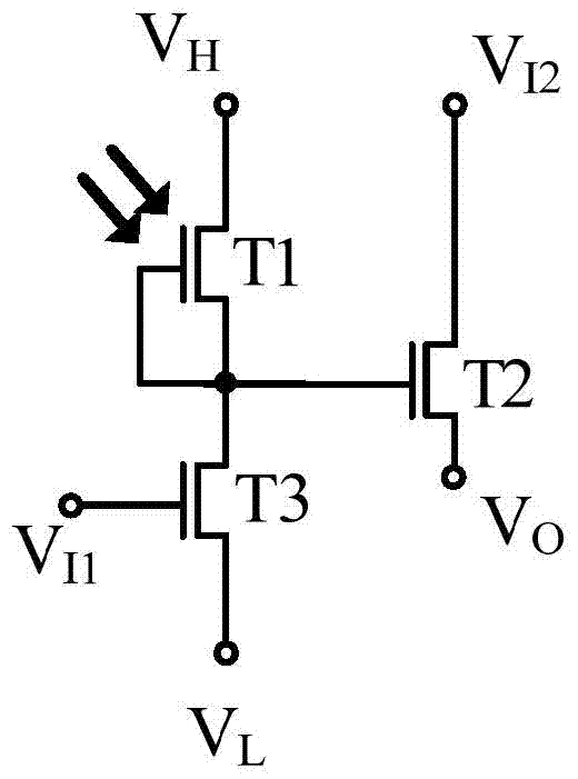
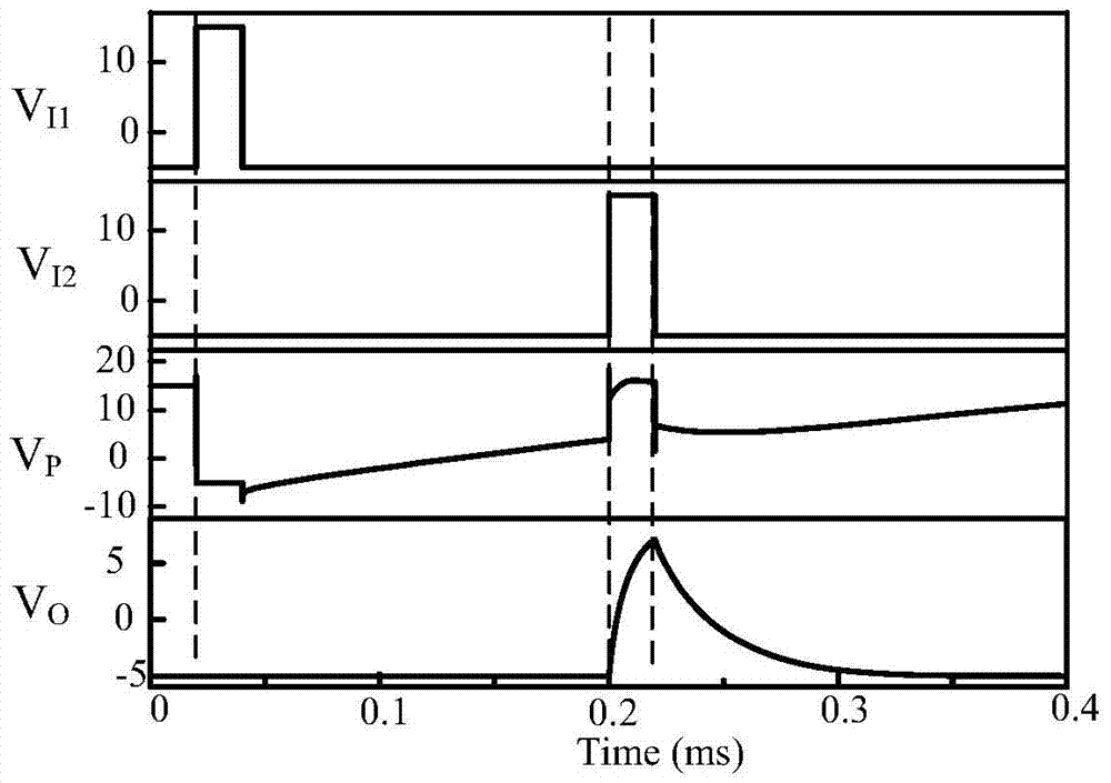
[0057] like figure 2 Shown is the structure diagram of the touch circuit unit of this embodiment, including:

[0058] The first pulse signal input terminal is used to input the first pulse signal V I1 ;

[0059] The second pulse signal input terminal is used to input the second pulse signal V I2 ;

[0060] The signal output terminal is used to output the touch information voltage V O ;

[0061] Induction voltage node P;

[0062] Inductive branches used in series at the high-level end and the low-level end;

[0063] and readout transistor T2.

[0064] Wherein, the sensing branch includes: a sensing transistor T1 and a reset transistor T3. The sensing transistor T1 is connected in series with the first pole (such as the drain) and the second pole (such as the source) of the reset transistor T3 in a diode connection form to form a sensing branch. The sensing voltage node P is located between the sensing transistor T1 and the reset transistor ( T3 ). The control electro...

Embodiment 2

[0085] Figure 5Shown is the structural diagram of the touch circuit unit of this embodiment, which is different from the first embodiment in that the structure of the touch circuit unit of this embodiment further includes a capacitor C1. Both ends of the capacitor C1 are respectively coupled to the first pole (for example, the drain) and the second pole (for example, the source) of the reset transistor T3 .

[0086] By increasing the capacitor C1, the potential of the induction voltage node P can be made more stable, and in the induction stage, if there is no ultraviolet light, the noise voltage at the signal output terminal can be reduced more effectively.

Embodiment 3

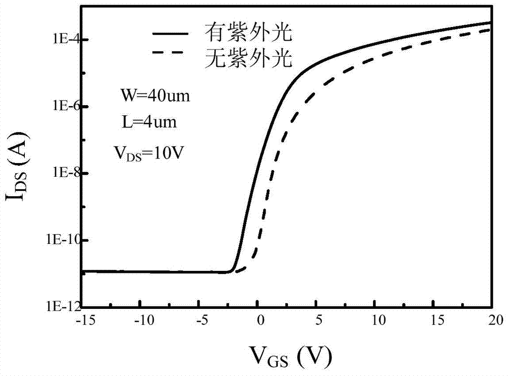
[0088] Please refer to Image 6 The difference between this embodiment and the above-mentioned embodiments is that, in the sensing phase, the readout transistor T2 also senses ultraviolet light information to adjust the threshold voltage of the readout transistor T2.

[0089] For the readout transistor T2, when there is no ultraviolet light outside, its threshold voltage value is relatively large, so the output voltage of the signal output terminal is relatively stable, and is not easily affected by the voltage feedthrough effect; and when there is ultraviolet light outside When irradiated, the threshold voltage of the readout transistor T2 decreases, so its conduction capability is stronger, and the signal output terminal is more likely to be charged and pulled up to a higher pulse high-level potential.

[0090] All in all, compared with the technical solution of Embodiment 1, the touch information voltage V output by the touch circuit unit of this embodiment O may be larger...


PUM


Abstract

The invention discloses a touch circuit unit suitable for an in-cell type touch technology. The touch circuit unit comprises an induction transistor, a reset transistor and a reading transistor. First the reset transistor responds to a first pulse signal to reset the touch circuit unit, the induction transistor senses touch movement of outside invisible light, and finally induction information is output through the reading transistor. The touch circuit unit can generate a wide-amplitude current or voltage signals to a peripheral circuit according to the invisible light low in strength and is high in noise resistance. A touch circuit distributed in a pixel circuit matrix, a touch display panel designed on the basis of the touch circuit and a touch display device are further disclosed simultaneously.

Description

technical field [0001] The present application relates to the field of touch screens, in particular to a touch circuit and its unit, a touch display panel and its device. Background technique [0002] In recent years, touch screen technology has developed rapidly. Touch screen technology can provide a good human-computer interaction interface, so it is more and more widely used in consumer and industrial electronic products. For consumer electronics products such as mobile phones, touch screen design requirements include: responsiveness, low noise, and easy integration with display panels. Therefore, the display panel with the touch function still maintains the characteristics of light weight, thin thickness, high display contrast, and low power consumption. [0003] Touch screen technology is mainly divided into out-cell type and in-cell type. In the existing out-cell type, a film layer with a touch control function is combined with a display panel in an adhesive manner....

Claims


Application Information

Patent Timeline
IPC IPC(8): G06F3/041
Inventor 张盛东廖聪维胡治晋李君梅李文杰
Owner PEKING UNIV SHENZHEN GRADUATE SCHOOL
Why Eureka
Try Eureka