Method for planarization of double faces of mercury-cadmium-telluride infrared material device

An infrared material, mercury cadmium telluride technology, applied in the field of infrared detection, can solve problems such as wafer deformation, and achieve the effect of improving flatness

Inactive Publication Date: 2014-04-30
11TH RES INST OF CHINA ELECTRONICS TECH GROUP CORP
View PDF2 Cites 3 Cited by
  • Summary
  • Abstract
  • Description
  • Claims
  • Application Information

AI Technical Summary

Problems solved by technology

[0003] In view of the above analysis, the present invention aims to provide a double-sided planarization method for mercury cadmium telluride infrared material devices to solve the problem of wafer deformation caused by multiple bonding during step-by-step polishing in the prior art

Method used


Image

  • Method for planarization of double faces of mercury-cadmium-telluride infrared material device

Examples


Embodiment 1

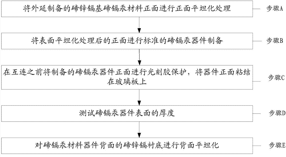
[0035] The HgCdTe material wafer size is 30mm×25mm, and the surface is ground with a diamond grinding wheel to remove the thickness of 3 microns, and then the grinding wheel damage is removed; after the standard HgCdTe device process, the photoresist is protected and then adhered to the glass plate with wax. The thickness difference between the maximum value and the minimum value of the test thickness is 7 microns, and the thickness is removed by diamond grinding wheel grinding to remove 10 microns, and the flatness of the tested mercury cadmium telluride device is 1.75 microns, which meets the interconnection requirements.

Embodiment 2

[0037] The HgCdTe material wafer size is 30mm×25mm, and the surface is ground with a diamond grinding wheel to remove a thickness of 2.5 microns, and then the grinding damage of the grinding wheel is removed; after the standard HgCdTe device process, the photoresist is protected and then adhered to the glass plate with wax. The thickness difference between the maximum value and the minimum value of the test thickness is 6 microns, and the thickness is removed by diamond grinding wheel grinding to remove 10 microns, and the flatness of the HgCdTe device is 1.55 microns, which meets the interconnection requirements.

Embodiment 3

[0039] The HgCdTe material wafer size is 36mm×38mm, and the surface is ground with a diamond grinding wheel to remove a thickness of 5 microns, and then the grinding wheel grinding damage is removed; after standard HgCdTe device technology, the photoresist is used to protect and adhere to the glass with epoxy glue On the board, the thickness difference between the maximum value and the minimum value of the test thickness is 11 microns, and the thickness of 15 microns is removed by single-point diamond turning, and the flatness of the HgCdTe device is 1.95 microns, which meets the interconnection requirements.


PUM


Abstract

The invention discloses a method for planarization of the double faces of a mercury-cadmium-telluride infrared material device. The method comprises the steps that A, front face planarization treatment is conducted on the front face of a cadmium-zinc-telluride-base mercury-cadmium-telluride material prepared through epitaxy; B, the front face obtained after the surface planarization treatment is used for standard preparation of a mercury-cadmium-telluride device; C, before interconnection is conducted, photoresist protection is conducted on the front face of the prepared mercury-cadmium-telluride device and the front face of the device adheres to a glass board; D, the thickness of the surface of the mercury-cadmium-telluride device is tested; E, back face planarization treatment is conducted on a cadmium-zinc-telluride substrate on the back face of the device. According to the method for planarization of the double faces of the mercury-cadmium-telluride infrared material device, the planeness of the mercury-cadmium-telluride material device is greatly improved and the requirement for interconnection between a large-area-array infrared focal plane device and a Si reading circuit is satisfied.

Description

technical field [0001] The invention relates to the technical field of infrared detection, in particular to a double-sided flattening method for mercury cadmium telluride infrared material devices. Background technique [0002] Infrared devices are generally prepared by growing a thin film on the surface of a CdZnTe substrate by liquid phase epitaxy (LPE), molecular beam epitaxy (MBE) or metal organic compound deposition (MOCVD), and then making a p-n junction. Since the CdZnTe substrate is a soft and brittle material, its processing technology cannot be processed by double-sided polishing. Instead, it is bonded to the glass substrate and polished on the A side first, and then the A side is protected after meeting the processing requirements. Post-bond, then polish side B. This step-by-step polishing method needs to bond the wafer multiple times during polishing. Since the bonding process will cause deformation of the wafer surface, the flatness of the CdZnTe substrate prep...

Claims


Application Information

Patent Timeline
Patent Type & Authority Applications(China)
IPC IPC(8): H01L31/18H01L21/304
CPCH01L31/1832H01L31/186Y02P70/50
Inventor 李春领王春红秦艳红
Owner 11TH RES INST OF CHINA ELECTRONICS TECH GROUP CORP
Why Eureka
Try Eureka