Laser direct writing exposure device based on stimulated light emission loss

A technology of stimulated emission of light and laser direct writing, which is applied in the field of optical exposure and can solve problems such as unconsidered, enhanced resolution, and high requirements for thin films

Active Publication Date: 2014-05-07
BEIJING GUOWANG OPTICAL TECH CO LTD
View PDF7 Cites 17 Cited by
  • Summary
  • Abstract
  • Description
  • Claims
  • Application Information

AI Technical Summary

Problems solved by technology

Most importantly, there is an unavoidable problem with the above-mentioned technologies: any imaging system cannot exceed the Abbe diffraction limit
However, this method has high requirements for the film to be produced, and it is very difficult to precisely control the photoresist in the process.
In addition, in the above-mentioned technologies, how to enhance the resolution while improving the depth of focus has not been considered, but in the optical exposure etching technology, two factors need to be considered at the same time

Method used


Image

  • Laser direct writing exposure device based on stimulated light emission loss
  • Laser direct writing exposure device based on stimulated light emission loss
  • Laser direct writing exposure device based on stimulated light emission loss

Examples


specific Embodiment

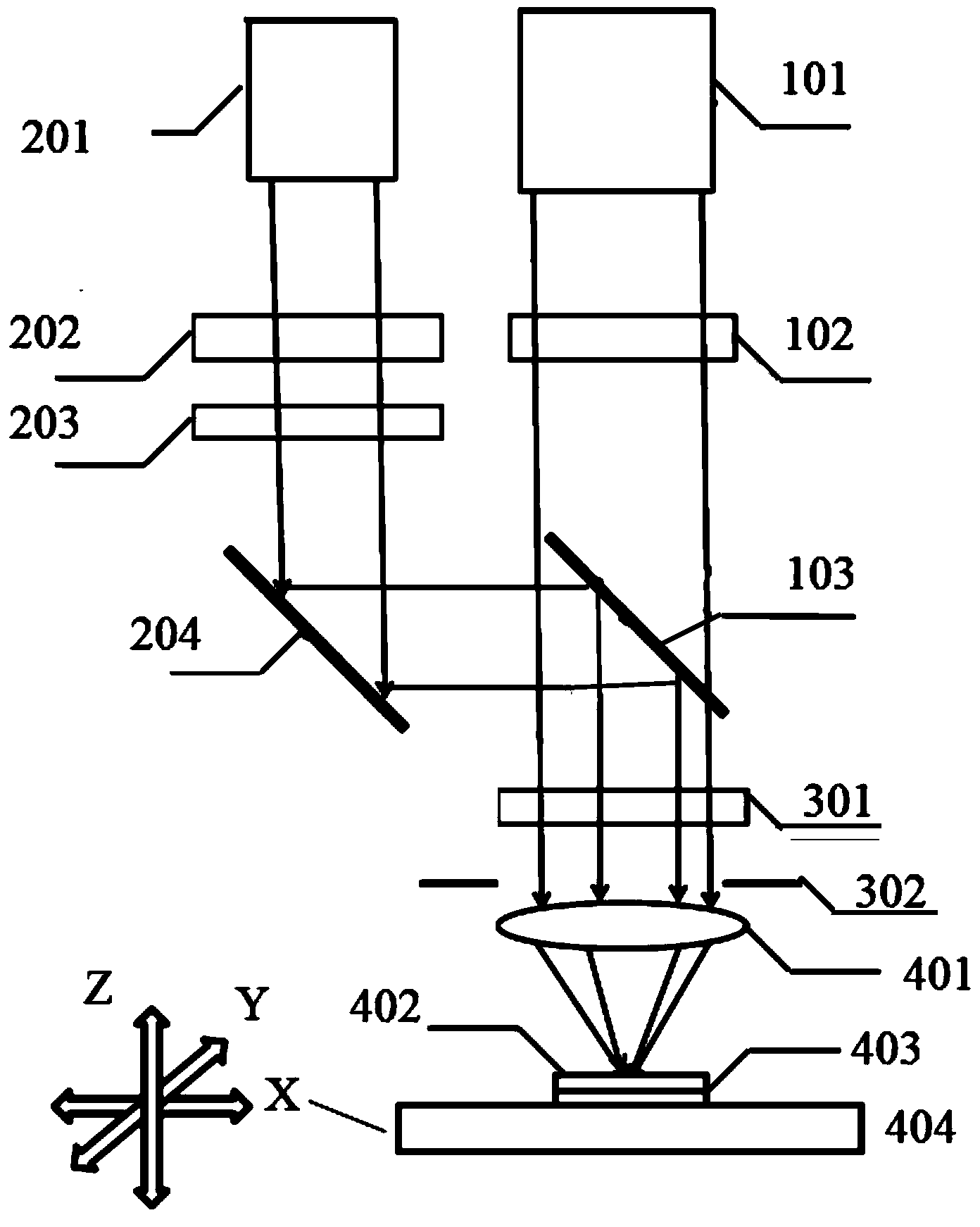
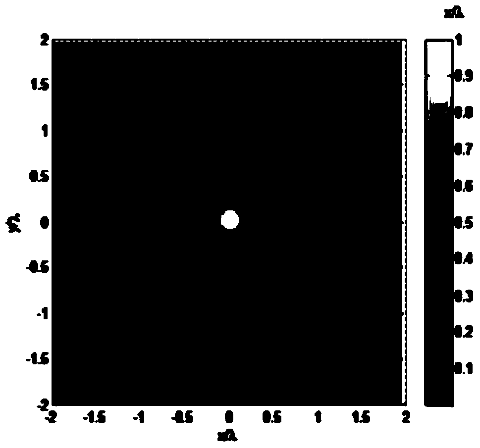
[0076] In this specific embodiment, the numerical aperture NA=0.95 of selecting high numerical aperture achromatic objective lens 401; The phase control parameter σ=30 of phase type zone plate 301 -5 , f=12; beam relative size δ 0 =1.2; the radius ratio of the amplitude-type zone plate 302 is η=0.92, and η is the ratio of the radius of the central light-transmitting region of the amplitude-type zone plate to the radius of the outer circle; the absorption factor ξ=100. The obtained light field on the focal plane is shown in Figure 3, where Figure 3a is the light field distribution formed by the excitation light source on the focal plane, and the coordinate axis in the figure is in wavelength. said Figure 3b is the light field distribution of the de-excitation light on the focal plane, and the center of the field of the de-excitation light on the focal plane is a dark field. Therefore, the ring-shaped area of ​​the photoresist irradiated by the de-excitation light cannot co...


PUM


Abstract

The invention discloses a laser direct writing exposure device based on stimulated light emission loss. The laser direct writing exposure device is characterized by comprising an excitation light source, a de-excitation light source, a first space light modulator, a second space light modulator, a half wave plate group, a dichroscope, a phase position type wave zone plate, an amplitude type wave zone plate, a high numerical value aperture achromatic objective and a three-dimension scanning platform. The laser direct writing exposure device provided by the invention can realize the optical exposure of high resolution and long focus depth.

Description

technical field [0001] The invention belongs to the field of optical exposure, in particular to a laser direct writing exposure device based on laser emission loss. Background technique [0002] With the continuous improvement of VLSI integration, the projection lithography technology, which is the key technology of integrated circuit manufacturing, has also developed rapidly. Continuously improving the resolution and depth of focus of the projection lithography system has always been the focus of research by researchers. Optical exposure technology is mainly to shorten the exposure wavelength of the lithography machine and increase the numerical aperture of the lithography objective lens as an effective means to improve the resolution of the lithography machine, but at the same time, the depth of focus of the projection objective lens will be sharply reduced. The current international mainstream deep ultraviolet lithography (DUVL) technology uses off-axis illumination to o...

Claims


Application Information

Patent Timeline
Patent Type & Authority Applications(China)
IPC IPC(8): G03F7/20
Inventor 朱菁黄惠杰杨宝喜宋强张方王键陈明李璟
Owner BEIJING GUOWANG OPTICAL TECH CO LTD
Why Eureka
Try Eureka