Display panel mother board and preparation method thereof

A technology for display panels and motherboards, which is applied in the fields of printed circuit manufacturing, multilayer circuit manufacturing, semiconductor/solid-state device manufacturing, etc., and can solve the problems of inability to release stress, film layer pattern shift, shrinkage or expansion instability And other issues

Inactive Publication Date: 2014-05-07
BEIJING BOE OPTOELECTRONCIS TECH CO LTD +1
View PDF5 Cites 15 Cited by
  • Summary
  • Abstract
  • Description
  • Claims
  • Application Information

AI Technical Summary

Problems solved by technology

After etching, it cannot play the role of stress relief
Therefore, after the process of forming the passivation layer and the gate insulating layer, the glass substrate is affected by the internal stress of the large-area electrical insulating layer such as the pa

Method used


Image

  • Display panel mother board and preparation method thereof
  • Display panel mother board and preparation method thereof
  • Display panel mother board and preparation method thereof

Examples


Embodiment 1

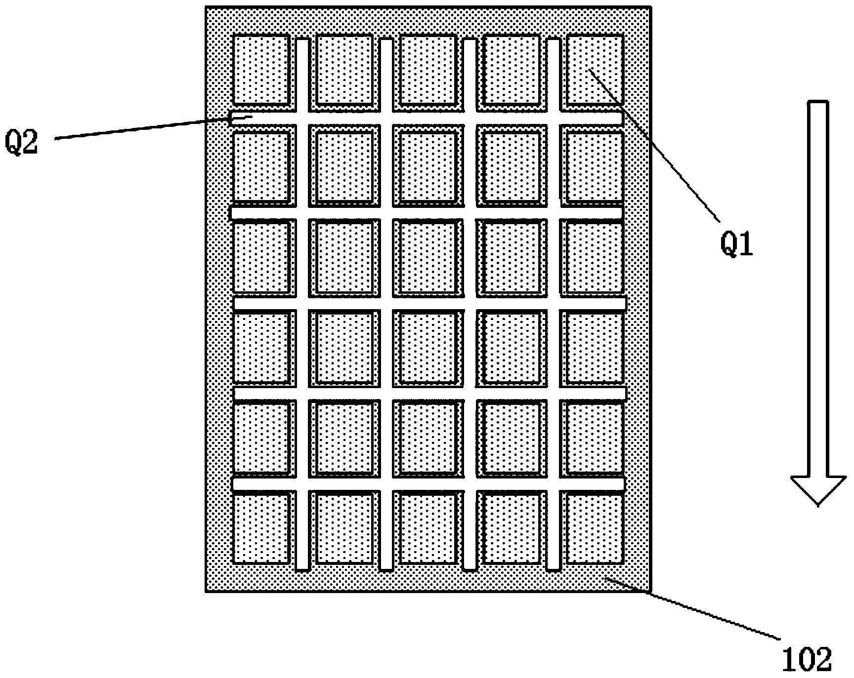
[0026] Such as figure 1 As shown, the present embodiment provides a display panel motherboard, which includes: display panel regions Q1 arranged at intervals, and a pre-cut region Q2 adjacent to the display panel regions Q1. Wherein, the display panel area Q1 corresponds to the location of the display panel, and the pre-cutting area Q2 corresponds to the location of the cutting line. In the motherboard of the display panel, at least part of the electrical insulating layer 102 disposed in the pre-cut area Q2 is removed.

[0027] Since at least part of the electrical insulating layer 102 located in the pre-cut area Q2 in the motherboard of the display panel of this embodiment is removed, the internal stress of the electrical insulating layer 102 can be well released, so that it can be well avoided. The influence of the greater stress inside the electrical insulating layer 102 on other film layers above or below the electrical insulating layer 102 can further affect the deviatio...

Embodiment 2

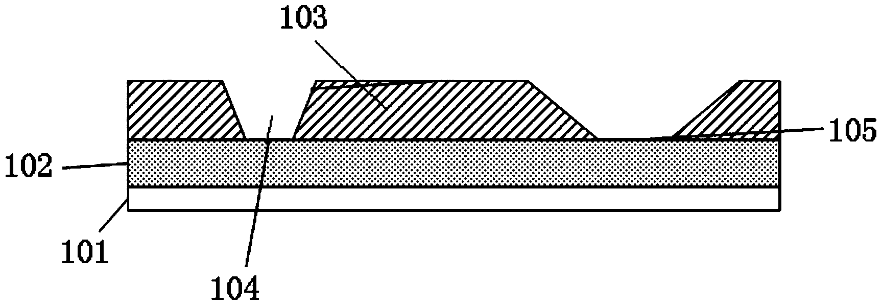
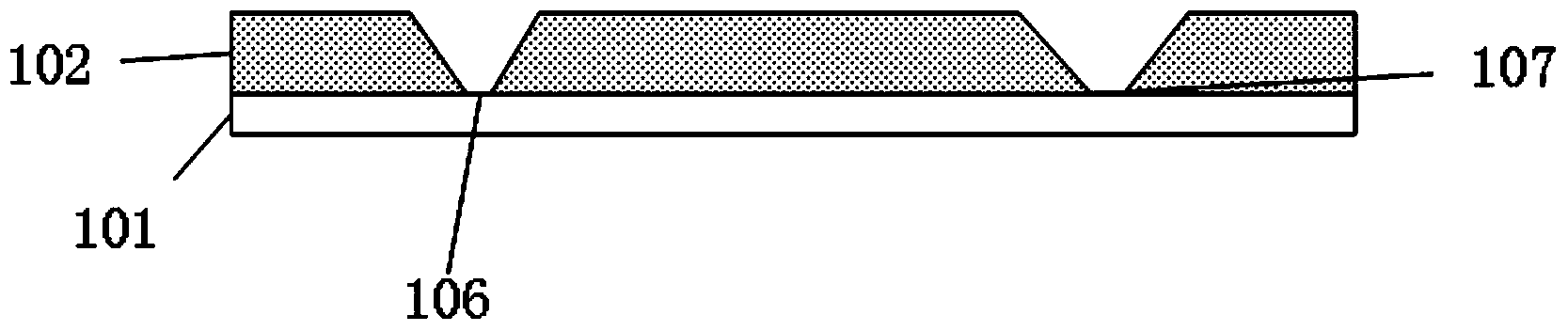
[0032] Such as Figure 2a and 2b As shown, this embodiment provides a method for preparing a display panel motherboard, the display panel motherboard comprising: display panel regions arranged at intervals, and a pre-cut region adjacent to the display panel, which includes the following steps:

[0033] Form a layer of electrical insulation layer film 102 on the substrate 101, and coat photoresist 103 on the electrical insulation layer film 102, expose and develop the photoresist, and contact the photoresist 104 of the via hole area and the electrical field of the pre-cut area. The photoresist 105 in the area where the insulating layer will be removed is removed, such as Figure 2a shown in .

[0034] Certainly, the step of forming contact vias may be synchronized with the above steps, or may be independent. When multiple electrical insulating layers 102 are included, the contact vias of each layer may be formed separately first, and then the electrical insulating layers 102...


PUM

PropertyMeasurementUnit
Angleaaaaaaaaaa

Abstract

The invention provides a display panel mother board and a preparation method thereof, belongs to the field of display techniques and solves the problem that other graphs in the display panel mother board offset due to large inside stress of electrical insulation layers in the existing display panel mother board. The display panel mother board comprises a plurality of display panel regions arranged at intervals and precutting regions adjacent to the display panel regions, wherein at least parts of the electrical insulation layers arranged in the precutting regions in the display panel mother board are removed.

Description

technical field [0001] The invention belongs to the field of display technology, in particular to a display panel motherboard and its [0002] Preparation. Background technique [0003] In the field of display technology, display devices are widely used in modern digital information equipment due to their advantages of small size, low power consumption, no radiation, and high resolution. [0004] The display device includes a display panel, wherein the display panel is formed by cutting two display panel motherboards (array substrate motherboard and color filter substrate motherboard) into boxes, wherein the display panel motherboard is provided with cutting line (the location of the cutting line is the pre-cut area on the display panel motherboard), the cutting line divides the display panel motherboard into multiple display panels (the location of the display panel is the display panel area of ​​the display panel motherboard), and according to the cutting After the cutti...

Claims


Application Information

Patent Timeline
IPC IPC(8): H01L27/12H01L21/77
CPCH01L27/1218H01L27/1288H01L27/1214H01L27/124H01L27/1248H05K1/0296H05K3/0017H05K3/0073H05K3/46
Inventor 杨光沈鹏王晏酩
Owner BEIJING BOE OPTOELECTRONCIS TECH CO LTD
Why Eureka
Try Eureka