Improved gradient freeze GaAs single crystal growing method

A gradient solidification, improved technology, applied in the direction of single crystal growth, single crystal growth, crystal growth, etc., can solve problems such as cumbersome

Inactive Publication Date: 2014-05-14
KUNSHAN DINGJING GALLIUM CRYSTAL MATERIAL
View PDF5 Cites 16 Cited by
  • Summary
  • Abstract
  • Description
  • Claims
  • Application Information

AI Technical Summary

Problems solved by technology

Therefore, each heating system must be care

Method used


Image

  • Improved gradient freeze GaAs single crystal growing method
  • Improved gradient freeze GaAs single crystal growing method

Examples


Embodiment 1

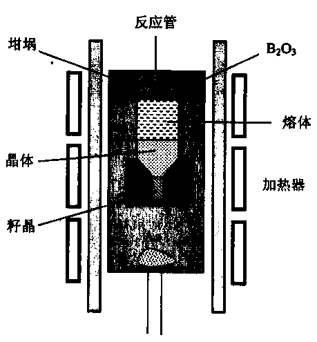
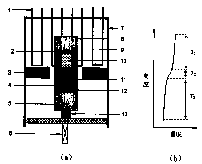
[0020] Growth of undoped GaAs single crystals. Put 4.0 kg of high-purity GaAs polycrystalline raw material into a PBN crucible with a diameter of 4 inches, and a seed crystal with a orientation and a diameter of 10 mm was placed on the bottom of the crucible in advance. Then the crucible was placed in a crystal growth furnace, the furnace temperature was controlled at 1255°C, and seed growth was started after the temperature was kept constant for 12 hours. The crystal growth temperature gradient was 7°C / cm, and the growth cycle was 7 days. After the growth, anneal at 850°C for 10 hours in a constant temperature zone, and slowly cool down to room temperature to obtain GaAs crystals with bright and non-wetting surfaces.

Embodiment 2

[0022] Growth of low Si-doped GaAs single crystals. 3.8 kg of high-purity GaAs polycrystalline raw material and 55 mg of Si were mixed into a PBN crucible with a diameter of 4 inches, and a seed crystal with a diameter of 12 mm and a orientation was placed at the bottom of the crucible. Put the PBN crucible into the crystal growth furnace, control the temperature of the furnace at 1255°C, and start the inoculation growth after 12 hours of constant temperature. The crystal growth temperature gradient was 10°C / cm, and the growth cycle was 7 days. After the growth is completed, anneal at 900°C for 12 hours in a constant temperature zone, and slowly cool down to room temperature to obtain a 4-inch low-Si-doped GaAs crystal with a bright and non-wetting surface.

Embodiment 3

[0024] Growth of heavily Si-doped GaAs single crystals. 3.5 kg of high-purity GaAs polycrystalline raw material was mixed with 80 mg Si and placed in a 4-inch-diameter PBN crucible. A -oriented seed crystal with a diameter of 10 mm was placed at the bottom of the crucible. Put the PBN crucible into the crystal growth furnace, control the temperature of the furnace at 1260°C, and start the inoculation growth after 12 hours of constant temperature. The crystal growth temperature gradient was 15°C / cm, and the growth cycle was 7 days. After the growth is completed, anneal at 950°C for 12 hours in a constant temperature zone, and slowly cool down to room temperature to obtain a 4-inch heavily Si-doped GaAs crystal with a bright and non-wetting surface.

[0025]


PUM


Abstract

The invention provides an improved gradient freeze GaAs single crystal growing method. According to the method, a traditional vertical gradient freeze (VGF) or vertical Bridgman (VB) crystal growing device is improved. The improved gradient freeze GaAs single crystal growing method is characterized in that a heating system is installed at the top of a crystal growing furnace and heating elements are a set of series-connection U-shaped silicomolybdic bars. The distribution curve of temperatures in a furnace body is formed through a heat insulation plate. GaAs raw materials are molten in a high-temperature area above the heat insulation plate and melt grows in a crystallizing mode in a temperature gradient area formed by the heat insulation plate. Obtained crystals are moved to the space below the heat insulation plate through a descending device, and high-temperature in-situ annealing is conducted to release thermal stress. GaAs single crystals grown by the adoption of the technology have the advantages of being low in dislocation, large in size, small in thermal stress and the like.

Description

technical field [0001] The invention relates to an improved gradient solidification GaAs single crystal growth method, which belongs to the field of crystal growth. Background technique [0002] The GaAs compound belongs to the second-generation semiconductor of the III-V group, and its status is second only to the Si material. Compared with Si, GaAs has a larger band gap, higher electron mobility and higher saturation velocity, so electronic devices made of GaAs work faster, have a higher operating frequency and have a wider operating temperature range than corresponding Si devices. This makes GaAs replace Si as the most important semiconductor material for making modern ultra-high-speed electronic devices and circuits. In recent years, GaAs materials and related industries have developed rapidly, with an annual growth rate of more than 20%. In 2010, its output value exceeded 10 billion US dollars. In the next few decades, the GaAs industry will still maintain a strong gr...

Claims


Application Information

Patent Timeline
IPC IPC(8): C30B29/42C30B11/00
Inventor 金敏徐家跃何庆波
Owner KUNSHAN DINGJING GALLIUM CRYSTAL MATERIAL
Why Eureka
Try Eureka