CdTe single crystal and CdTe polycrystal, and method for preparation thereof

a single crystal and polycrystal technology, applied in the direction of polycrystalline material growth, crystal growth process, under protective fluid, etc., can solve the problems of low sensitivity of radiation detectors, inability to realize a cdte single crystal whose chlorine concentration is not more than 5 ppmwt and resistivity not less than 1.010sup>9 /sup>9 /sup>cm, and poor production efficiency compared with th

Active Publication Date: 2007-05-01
JX NIPPON MINING & METALS CORP
View PDF17 Cites 5 Cited by
  • Summary
  • Abstract
  • Description
  • Claims
  • Application Information

AI Technical Summary

Benefits of technology

[0022]Thereby, the inventors have become convinced that the material of the sealed container (inner container 4a) at the time of synthesizing a CdTe polycrystal affects the resistivity of a CdTe single crystal using the CdTe polycrystal as a raw material, and have found that the resistivity of a CdTe single crystal can be made high without doping excess chlorine by which uses pBN as the material of the container.

Problems solved by technology

Thereby, there is a problem such that the sensitivity of a radiation detector becomes low.
However, with the technique in the Japanese Patent Laid-Open Publication No. 5-283729, a CdTe single crystal having high resistance can be produced compared with the producing methods of utilizing the THM in the earlier technology, however, it is unable to realize a CdTe single crystal whose chlorine concentration is not more than 5 ppmwt and resistivity not less than 1.0×10⁹ Ω·cm cannot be realized.
Further, generally, in the growth of single crystal according to the THM, the growth rate is extremely slow as approximately 5 mm per day, so that there is a disadvantage that its production efficiency is bad compared with the VGF method or the like.
Thus, with the methods for producing a CdTe single crystal by the THM in the earlier technology, it is difficult to produce a CdTe single crystal having high purity and high resistance with sufficient productivity.

Method used


Image

  • CdTe single crystal and CdTe polycrystal, and method for preparation thereof
  • CdTe single crystal and CdTe polycrystal, and method for preparation thereof
  • CdTe single crystal and CdTe polycrystal, and method for preparation thereof

Examples


Embodiment Construction

[0030]Hereinafter, a preferred embodiment of the present invention will be explained on the basis of the drawings.

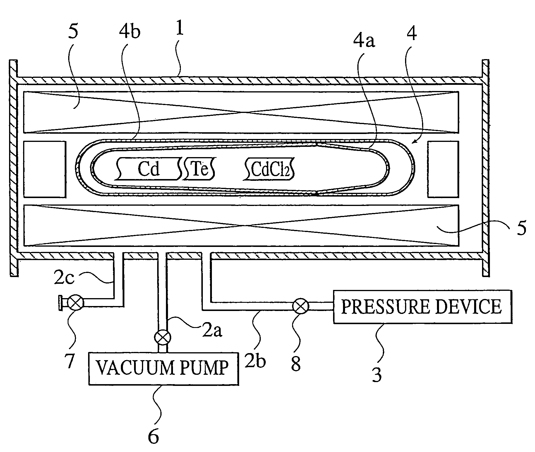
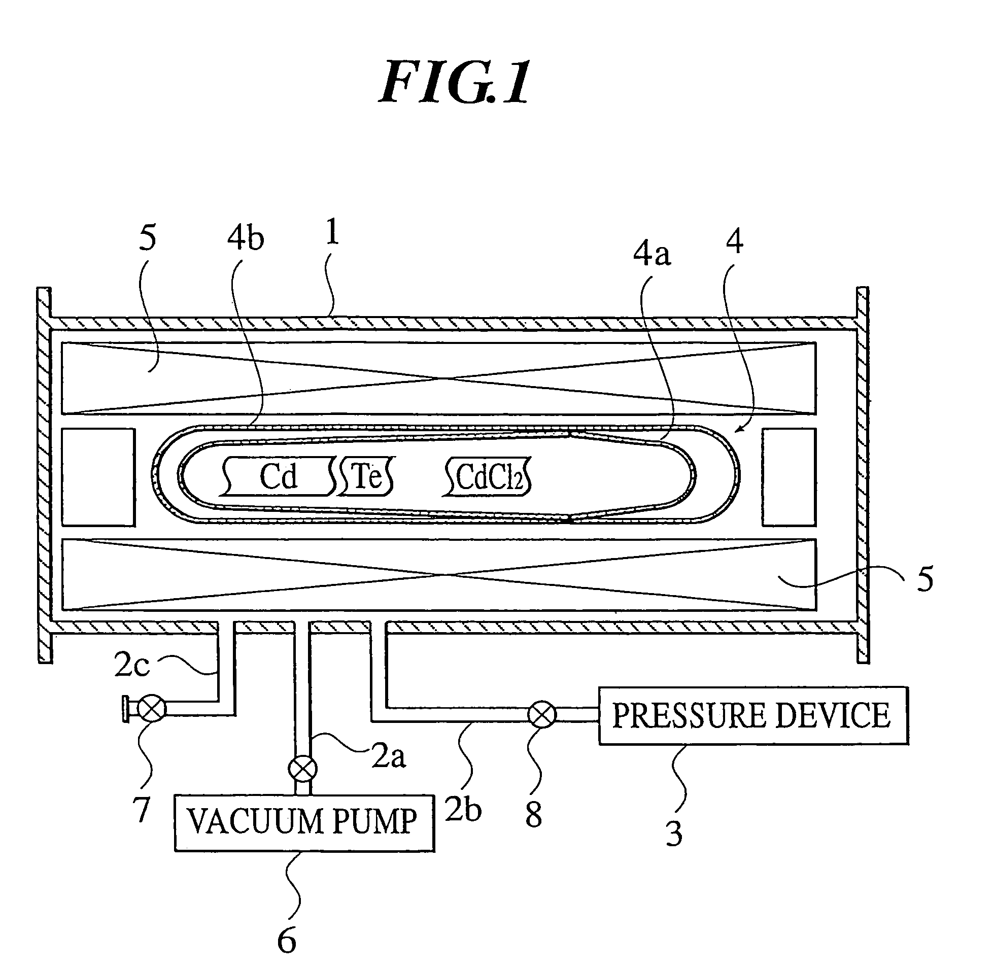
[0031]At first, a method for synthesizing a CdTe polycrystal by using an apparatus in FIG. 1 will be explained. FIG. 1 is a view schematically showing a construction of the apparatus used for synthesis of the CdTe polycrystal of the embodiment.

[0032]In FIG. 1, the reference numeral 1 is a high pressure container. A vacuum pump 6 is connected to the high pressure container 1 through a pipe 2a, and a pressure device 3 is connected to the same through a pipe 2b. After discharging air in the high pressure container 1 by the vacuum pump 6, N2 gas or the like is put into the high pressure container 1 by the pipe 2b so as to substitute the internal gas. The N2 gas or the like is further pressed into the high pressure container 1 by the pressure device 3 so as to make it possible to adjust the pressure in the high pressure container 1.

[0033]Further, a third pipe 2c is connected ...


PUM

PropertyMeasurementUnit
resistivityaaaaaaaaaa
carrier concentrationaaaaaaaaaa

Abstract

A CdTe single crystal, wherein chlorine concentration in the crystal is between 0.1 and 5.0 ppmwt and resistivity at room temperature is not less than 1.0×10⁹ Ω·cm is obtained by growing the crystal according to one of a vertical gradient freezing method, a horizontal gradient freezing method, a vertical Bridgman method, a horizontal Bridgman method, and a liquid encapsulated Czochralski method by using a CdTe polycrystal, in which 50 to 200 ppmwt of chlorine is doped, as a raw material.

Description

FIELD OF THE INVENTION[0001]The present invention relates to a Group II–VI compound semiconductor single crystal and a method for producing the same. In particular, the present invention relates to a CdTe system compound semiconductor single crystal having high resistance, which is useful as a substrate for a semiconductor device, such as a radiation detector or the like, and to a CdTe polycrystal which becomes a raw material of the above-described CdTe single crystal, and to a method for producing the same.BACKGROUND ART[0002]Generally, CdTe single crystals having high purity and high resistance are suitable for substrates for semiconductor devices, such as radiation detector, IC tester and the like. It is known that the higher the resistance of the CdTe single crystal to be used is (for example, not less than 1.0×10⁹ Ω·cm), the more the device characteristic improves.[0003]In earlier technology, for producing a Group II–VI compound semiconductor single crystal, such as CdTe or the...

Claims


Application Information

Patent Timeline
Patent Type & Authority Patents(United States)
IPC IPC(8): C30B29/48C30B11/00C30B11/12C30B15/00C30B27/02
CPCC30B11/002C30B29/48C30B15/10
Inventor HIRANO, RYUICHI
Owner JX NIPPON MINING & METALS CORP
Why Eureka
Try Eureka