Copper-idium-selenium CuInSe solar cell and preparing method thereof
A solar cell, copper indium selenide technology, applied in circuits, electrical components, photovoltaic power generation and other directions, can solve problems such as cost reduction, difficulty in realizing industrialization, large waste of precious metals, etc. good adhesion
- Summary
- Abstract
- Description
- Claims
- Application Information
AI Technical Summary
Problems solved by technology
Method used
Image
Examples
Embodiment Construction
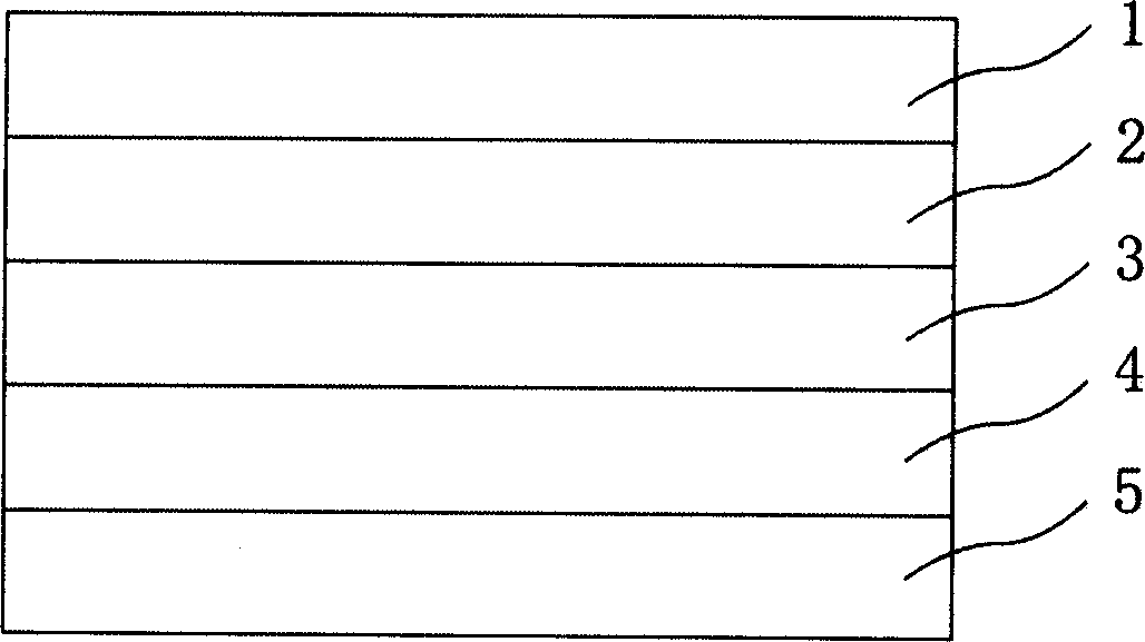
[0019] Such as figure 1 As shown, the high-efficiency copper indium selenium CuInSe described in the present invention 2 A solar cell consists of a lower electrode 1, a P-type copper indium selenium CuInSe 2 Sheet 2, transition layer CdS 3, N-type ZnO layer 4 and upper electrode 5. P-type Copper Indium Selenium CuInSe 2 The absorber layer is CuInSe 2 Single wafer, the lower electrode adopts Cu / Mo (copper / molybdenum) alloy.
[0020] In order to prepare the above-mentioned high-efficiency copper indium selenium CuInSe 2 Solar cell, preparation method of the present invention, comprises the following steps:
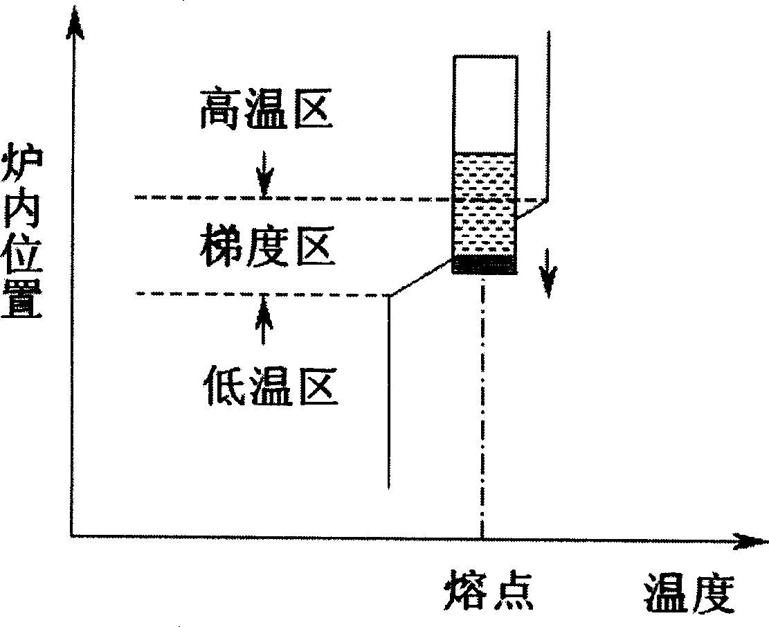
[0021] A certain amount of high-purity copper (99.999%), indium (99.999%) and selenium (99.999%) particles are removed from the surface oxide layer and then fully mixed according to the molar ratio of Cu:In:Se=1:1:2. Put it into a cleaned thick-walled quartz tube (crucible), which has been sealed at one end. Vacuum the quartz tube to 10 -6 , the other end of the quar...
PUM
 Abstract
Description
Claims
Application Information

