Transistor forming method

A technology of transistors and semiconductors, applied in the manufacture of transistors, semiconductor devices, semiconductor/solid-state devices, etc., can solve problems such as poor performance of transistors, achieve better isolation effects, improved and stable performance, and good device performance

Active Publication Date: 2014-05-14
SEMICON MFG INT (SHANGHAI) CORP
View PDF6 Cites 5 Cited by
  • Summary
  • Abstract
  • Description
  • Claims
  • Application Information

AI Technical Summary

Problems solved by technology

[0005] However, the transistor performance of the prior art

Method used


Image

  • Transistor forming method
  • Transistor forming method
  • Transistor forming method

Examples


Embodiment Construction

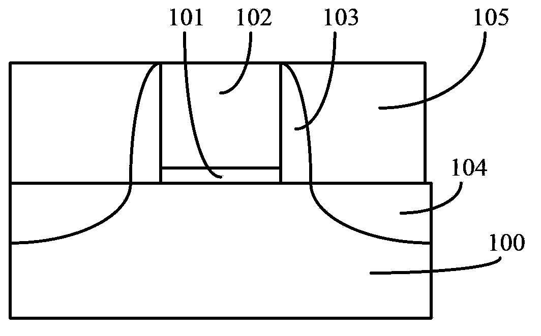
[0032] As mentioned in the background, the performance of the transistor with the high-K dielectric layer and the metal gate structure in the prior art is not good.

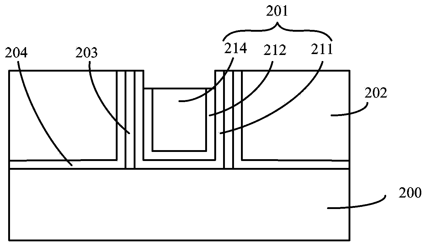
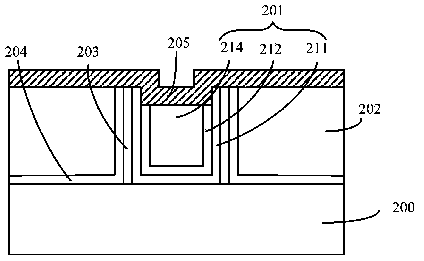
[0033] After research by the inventor of the present invention, please continue to refer to figure 1 , since the material of the metal gate layer 102 is metal, when the transistor is working, the prior art will directly apply an operating voltage to the top surface of the metal gate layer 102; however, directly to the metal gate layer When an operating voltage is applied to the top surface of the metal gate layer 102, the metal on the surface of the metal gate layer 102 will undergo metal electromigration under the action of an operating electric field, resulting in problems such as short circuit, short circuit or unstable performance of the device. In order to prevent the electromigration of metal on the top surface of the metal gate layer 102, the inventors of the present invention have found through research t...


PUM


Abstract

Provided is a transistor forming method which comprises: providing a semiconductor substrate, wherein a gate structure is disposed on the surface of the semiconductor substrate and comprises a gate dielectric layer and a gate electrode layer on the surface of the gate dielectric layer, the gate electrode layer is produced by metal material, and the surface of the semiconductor substrate also comprises a dielectric layer covering the sidewall of the gate structure; forming a sacrificial layer on the surfaces of the dielectric layer and the gate electrode layer, wherein the sacrificial layer comprises metal atoms different from the metal material of the gate electrode layer; diffusing the metal atoms in the sacrificial layer into the gate electrode layer by using thermal annealing technology in order to form a covering layer on the surface of the gate electrode layer; and removing the sacrificial layer residing at the surfaces of the covering layer and the dielectric layer. A formed transistor has excellent performance.

Description

technical field [0001] The invention relates to the technical field of semiconductor manufacturing, in particular to a method for forming a transistor. Background technique [0002] With the rapid development of integrated circuit manufacturing technology, the size of semiconductor devices in integrated circuits, especially MOS (Metal Oxide Semiconductor, metal-oxide-semiconductor) devices, has been continuously reduced to meet the miniaturization and development of integrated circuits. Integration requirements. In the process of continuous shrinking of the size of MOS transistor devices, the process of using silicon oxide or silicon oxynitride as the gate dielectric layer in the existing process is challenged. Transistors formed with silicon oxide or silicon oxynitride as the gate dielectric layer have some problems, including increased leakage current and diffusion of impurities, which affect the threshold voltage of the transistor and further affect the performance of se...

Claims


Application Information

Patent Timeline
IPC IPC(8): H01L21/336H01L21/28
CPCH01L21/28079H01L21/28088H01L29/4958H01L29/4966H01L29/66568
Inventor 洪中山
Owner SEMICON MFG INT (SHANGHAI) CORP
Why Eureka
Try Eureka