IGBT device and manufacturing method thereof

A device and drift region technology, used in semiconductor/solid-state device manufacturing, semiconductor devices, electrical components, etc., can solve problems such as reduction of on-state voltage drop

Inactive Publication Date: 2014-05-14
INST OF MICROELECTRONICS CHINESE ACAD OF SCI +1
View PDF5 Cites 6 Cited by
  • Summary
  • Abstract
  • Description
  • Claims
  • Application Information

AI Technical Summary

Problems solved by technology

Although the performance of IGBT devices has been greatly improved compared with traditional transistor devices, such as

Method used


Image

  • IGBT device and manufacturing method thereof
  • IGBT device and manufacturing method thereof
  • IGBT device and manufacturing method thereof

Examples


Embodiment Construction

[0045] As mentioned in the background section, in order to reduce the conduction loss of the IGBT, it is necessary to further reduce its conduction voltage drop.

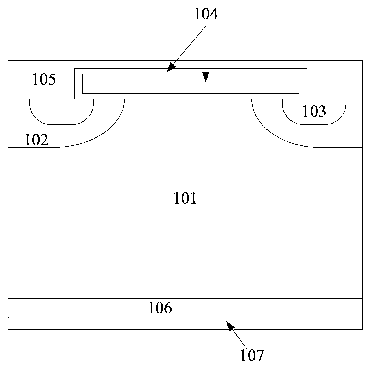
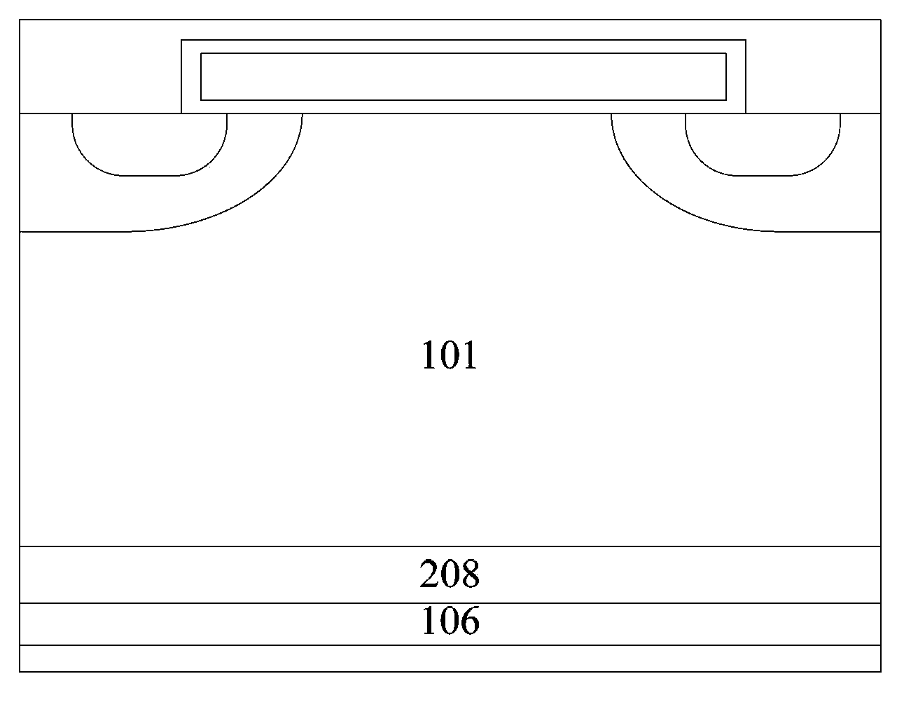
[0046] Taking the IGBT device with N-type planar gate structure as an example, it is divided into punch-through IGBT and non-punch-through IGBT, such as figure 1 as shown, figure 1 It is a structural schematic diagram of the non-punch-through IGBT device, including:

[0047] N-type lightly doped (N-) substrate, which includes: N-drift region 101, P-type well region 102 (generally P-type lightly doped) located on both shoulders of the drift region 101, and located on the N-type heavily doped (N+) source region 103 in the P-type well region 102;

[0048] a gate structure 104 on the surface of the substrate;

[0049] The source electrode 105 located on the surfaces of the well region 102 and the source region 103;

[0050] P-type heavily doped (P+) collector region 106 located in the lower surface of the substrate;...


PUM

PropertyMeasurementUnit
Thicknessaaaaaaaaaa

Abstract

The invention discloses an IGBT device and a manufacturing method thereof. The IGBT device comprises a substrate which comprises a drift region; a grid electrode structure and a source electrode structure which are arranged on the front surface of the substrate, and the source electrode structure comprises a trap region which is arranged in the surface of the drift region and a source region which is arranged in the surface of the trap region; a carrier storage layer which is arranged in the surface of the drift region and below the trap region, a gap is arranged between the carrier storage layer and the bottom part of the trap region, a doping type of the carrier storage layer and the doping type of the drift region are identical and doping concentration of the carrier storage layer is greater than that of the drift region; and a current collection region which is arranged on the back surface of the substrate, and the doping types of the current collection region and the drift region are opposite. The IGBT device is lower in conduction pressure drop and thus is low in conduction loss.

Description

technical field [0001] The invention relates to the technical field of semiconductor device manufacturing technology, and more specifically, relates to an IGBT device and a manufacturing method thereof. Background technique [0002] Insulated Gate Bipolar Transistor (IGBT for short) is a composite fully-controlled voltage-driven power semiconductor device composed of a bipolar transistor (BJT) and an insulated gate field effect transistor (MOSFET), and has a MOSFET Due to the high input impedance of the device and the high-speed switching characteristics of the power transistor (giant transistor, GTR for short), IGBT devices are widely used in AC motors, frequency converters, switching power supplies, lighting circuits, traction drives and other fields. [0003] The conduction voltage drop of a transistor device determines its conduction loss, and when the conduction voltage drop is small, its conduction loss is small. Although the performance of IGBT devices has been great...

Claims


Application Information

Patent Timeline
IPC IPC(8): H01L29/06H01L29/739H01L21/331
CPCH01L29/7398H01L29/66333H01L29/66348H01L29/7397
Inventor 谈景飞朱阳军褚为利张文亮王波
Owner INST OF MICROELECTRONICS CHINESE ACAD OF SCI
Why Eureka
Try Eureka