Technique method for patterning back surface of silicon wafer

A process method and graphic technology, applied in the manufacture of electrical components, electrical solid devices, semiconductor/solid devices, etc., can solve the problems of restricted processing technology, opacity of metal and silicon wafers, and inability to do backside processes, etc., to achieve reduction The effect of production costs

Active Publication Date: 2014-05-21
SHANGHAI HUAHONG GRACE SEMICON MFG CORP
View PDF3 Cites 11 Cited by
  • Summary
  • Abstract
  • Description
  • Claims
  • Application Information

AI Technical Summary

Problems solved by technology

The slides greatly restrict the follow-up processing technology. For example, organic film and glass cannot be electrostatically adsorbed, and the entire production line must be replaced with special adsorption equipment; metal and silicon wafers are opaque, and cannot be used for backside processing, etc.
Therefore, there is currently no effective method for a thin-sheet double-sided patterning process suitable for mass production, wherein the thin sheet is a silicon wafer with a thickness of <150 μm

Method used


Image

  • Technique method for patterning back surface of silicon wafer
  • Technique method for patterning back surface of silicon wafer
  • Technique method for patterning back surface of silicon wafer

Examples


Embodiment Construction

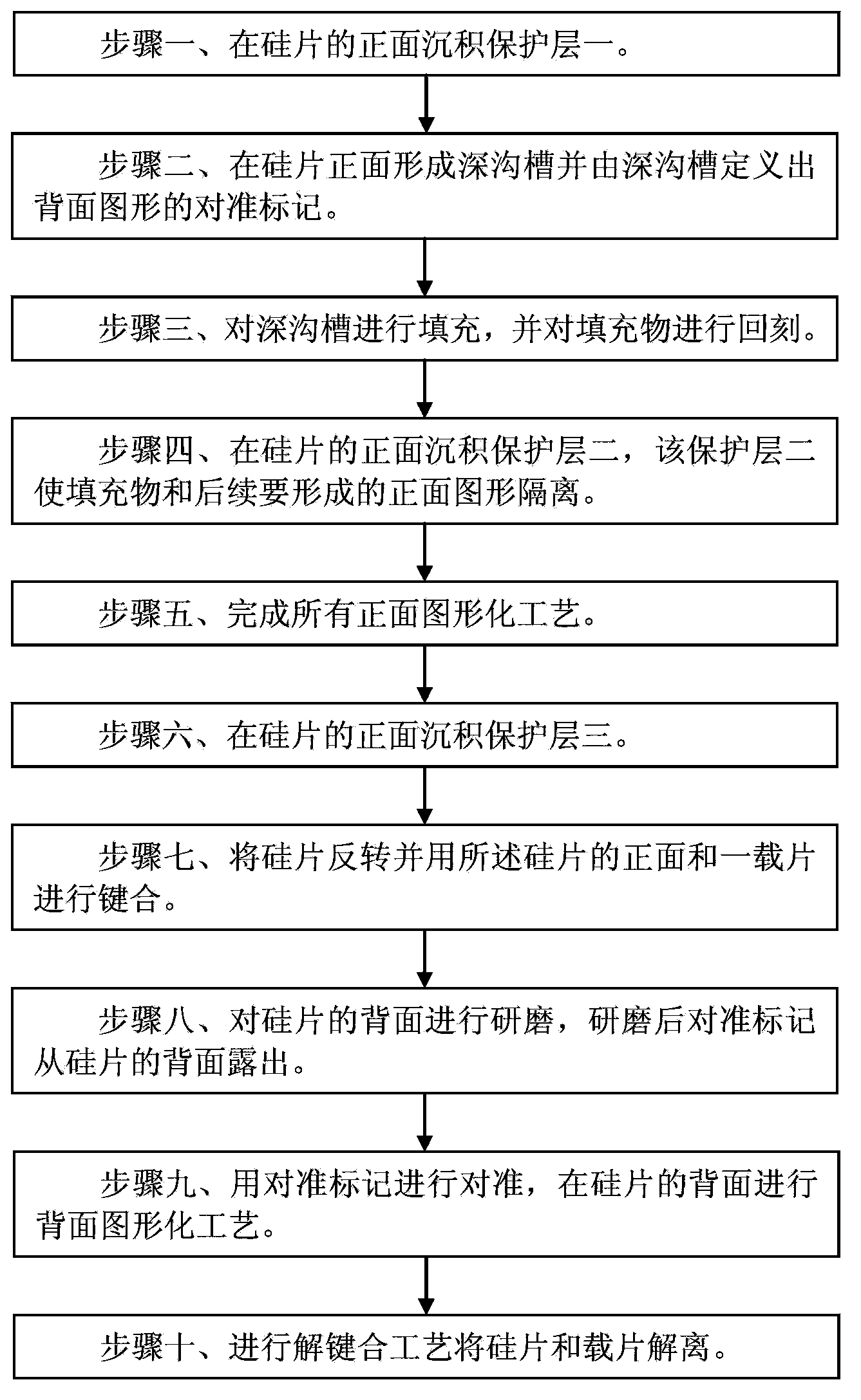
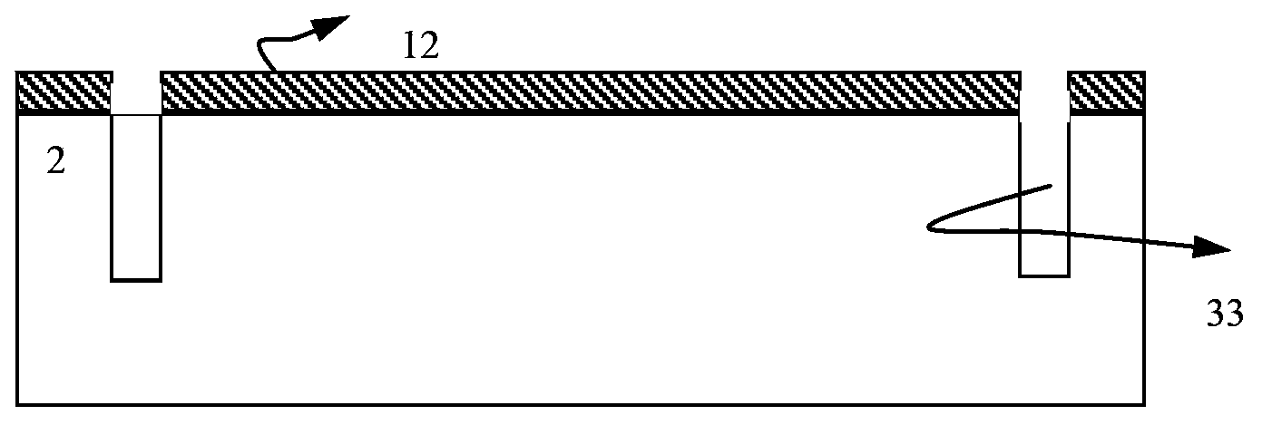
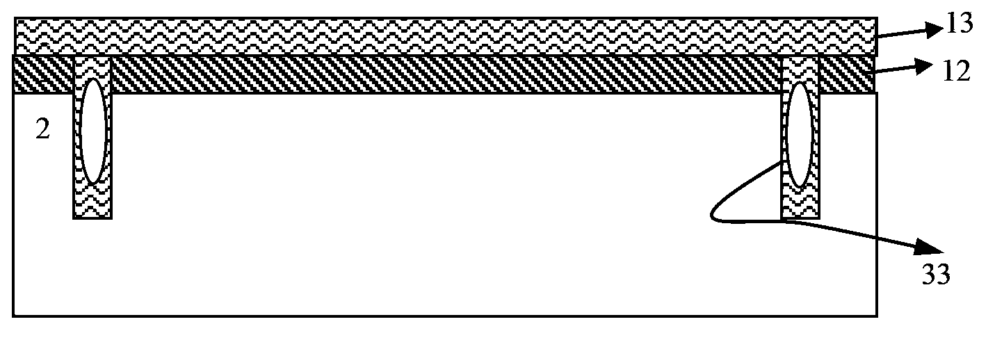
[0040] Such as figure 1 Shown is the flowchart of a method of the embodiment of the present invention; Figure 2A to Figure 2N Shown is a structural diagram of devices in each step of the method of Embodiment 1 of the present invention. In the first method of the embodiment of the present invention, an RC-IGBT with a rated breakdown voltage of about 1200V is taken as an example. The thickness of the silicon wafer 2 required by the device is 80 μm to 100 μm, and the front side of the silicon wafer 2 needs to form an IGBT device. The back side of sheet 2 needs to form a P / N distribution under the IGBT device pattern. Embodiment 1 of the present invention The process method for patterning the back side of a silicon wafer comprises the following steps:

[0041] Step 1, such as Figure 2A As shown, a silicon wafer 2 is provided, and the initial thickness of the silicon wafer 2 is 725 μm. A protective layer 12 is deposited on the front surface of the silicon wafer 2 .

[0042] ...


PUM

PropertyMeasurementUnit
depthaaaaaaaaaa
thicknessaaaaaaaaaa
thicknessaaaaaaaaaa

Abstract

The invention discloses a technique method for patterning the back surface of a silicon wafer. The technique method comprises: depositing a protective layer 1; forming a forming a deep trench and defining an aligning mark by using the deep trench; filling the deep trench; depositing a protective layer 2 in order to isolate a filler from a front-surface pattern to be formed subsequently; completing all front-surface patterning techniques; depositing a protective layer 3; reversing the silicon wafer and bonding the front surface of the silicon wafer with a carrier; grinding the back surface of the silicon wafer, wherein the aligning mark is exposed out of the back surface of the silicon wafer after the back surface of the silicon wafer is grinded; aligning by using the aligning mark and performing back surface patterning technique on the back surface of the silicon wafer; and performing a de-bonding technique for separating the silicon wafer from the carrier. According to the method provided by the invention, the aligning mark penetrates through the silicon wafer from the front surface to the back surface; when the back surface patterning technique is performed, an extra photoetching device and technique are not required to be added for achieving the aligning of the back-surface pattern and the front-surface pattern; and the production cost can be greatly decreased. In addition, the method is also compatible with a thin slice technique.

Description

technical field [0001] The invention relates to a process method for manufacturing semiconductor integrated circuits, in particular to a process method for patterning the back of a silicon wafer. Background technique [0002] For some power components, such as RC-IGBT (Reverse-Conductor IGBT, reverse interconnection IGBT), it is necessary to form a device structure on the front and back of the silicon wafer at the same time, so it is necessary to form patterns on both sides of the silicon wafer, and it is necessary to realize the front and back. Alignment of graphics on the back. [0003] In the existing process method, the alignment marks used for the alignment of the backside graphics are formed on the front side of the silicon wafer. After the front side process of the silicon wafer is completed, the silicon wafer is reversed and the backside process of the silicon wafer is carried out. During the process, the alignment marks formed on the front side of the silicon wafer...

Claims


Application Information

Patent Timeline
Patent Type & Authority Applications(China)
IPC IPC(8): H01L21/768
CPCH01L21/027H01L23/544H01L2223/54426
Inventor 王雷程晋广郁新举成鑫华
Owner SHANGHAI HUAHONG GRACE SEMICON MFG CORP
Why Eureka
Try Eureka