
A multi-source regulated resistive memory with a multi-layer film structure and its preparation method

A technology of resistive variable memory and multi-layer film, which is applied in semiconductor/solid-state device manufacturing, electric solid-state devices, semiconductor devices, etc., can solve the lack of semiconductor layer divergence, control the coefficient of electric resistive change, and the influence of MFS structure storage performance. And other issues

Inactive Publication Date: 2017-01-18
TIANJIN NORMAL UNIVERSITY
View PDF6 Cites 0 Cited by
  • Summary
  • Abstract
  • Description
  • Claims
  • Application Information

AI Technical Summary

Problems solved by technology

However, there has been a lack of direct experimental evidence on the influence of the accumulation and depletion of charges in the semiconductor electrode layer on the storage performance of the MFS structure, and there are huge gaps in the conclusions of different international research groups on the function of the semiconductor layer in the MFS structure. differences
Therefore, it is a huge challenge to properly describe the role of semiconductor thin films. The difficulty is that it is difficult to adjust the coefficient of resistive switching in situ by changing the amount of carriers in the semiconductor layer.

Method used


Image

  • A multi-source regulated resistive memory with a multi-layer film structure and its preparation method
  • A multi-source regulated resistive memory with a multi-layer film structure and its preparation method
  • A multi-source regulated resistive memory with a multi-layer film structure and its preparation method

Examples


Embodiment 1

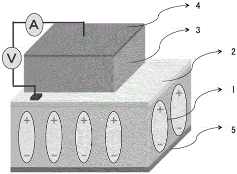
[0035] A multi-source regulated resistive memory with a multilayer film structure (see figure 1 ), including a ferroelectric single crystal substrate 1, a conductive lower electrode 2, a ferroelectric thin film layer or a heterojunction layer 3, an upper electrode thin film layer 4, and a gate electrode layer 5; it is characterized in that: the conductive lower electrode is set on the ferroelectric single crystal Between the substrate and the ferroelectric thin film layer or the heterojunction layer, the upper electrode thin film layer is arranged on the top layer, and the gate electrode layer is on the lowermost layer; the ferroelectric single crystal substrate is PMN-PT; the conductive lower electrode is La x Sr 1-x MnO 3 Manganese oxide, wherein the value of x is 0.1-0.2; the ferroelectric thin film layer or heterojunction layer is BaTiO 3 ; The upper electrode film layer or the gate electrode layer is Pt. The thickness of the ferroelectric single crystal substrate is 0....

Embodiment 2

[0037] A multi-source regulated resistive memory with a multilayer film structure (see figure 1 ), including a ferroelectric single crystal substrate, a conductive lower electrode, a ferroelectric thin film layer or a heterojunction layer, an upper electrode thin film layer, and a gate electrode layer; it is characterized in that: the conductive lower electrode is set on the ferroelectric single crystal substrate and the ferroelectric thin film Between layers or heterojunction layers, the upper electrode thin film layer is placed on the top layer, and the gate electrode layer is placed on the lowermost layer.

[0038] Ferroelectric single crystal substrate of the present invention is PMN-PT; Described conductive lower electrode is La x Ca 1-x MnO 3 Manganese oxide, wherein the value of x is 0.1-0.2; the ferroelectric thin film layer or heterojunction layer is BiFeO 3 Ferroelectric film; said upper electrode film layer or gate electrode layer is Au or Al. The thickness of t...

Embodiment 3

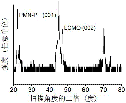
[0040] The structure of the transparent conductive oxide thin film with multi-layer film structure is: the substrate PMN-PT, the thickness is 0.5mm; the lower electrode layer is La 0.8 Ca 0.2 MnO 3 , with a thickness of 30nm; the thickness of the ferroelectric BTO film layer is 300nm; the thickness of the upper electrode layer Pt is 500nm; the thickness of the Ag gate electrode layer is 500nm. The deposition temperatures of the three-layer films are 750°C, 800°C and room temperature respectively, and the gases used in the deposition are O 2 (60Pa), O 2 (10Pa) and Ar gas (0.02Pa). figure 2 Shows BTO / La 0.8 Ca 0.2 MnO 3 / PMN-PT structure X-ray diffraction (XRD) patterns. The prepared samples were heated at 500 °C and high-purity O 2 Annealed under flow protection for 2 hours. The Ag gate electrode layer is prepared by thermal evaporation in a high vacuum chamber at room temperature.


PUM

PropertyMeasurementUnit
diameteraaaaaaaaaa
thicknessaaaaaaaaaa
thicknessaaaaaaaaaa

Abstract

The invention discloses a multi-field controllable resistive random access memory with a multi-layer film structure and a preparation method thereof. The resistive random access memory is composed of a piezoelectric substrate, a conductive lower electrode, a ferroelectric thin film layer, an upper electrode thin film layer and a gate electrode, wherein the piezoelectric substrate is made from a PMN-PT (Plumbum Magnesium Niobate ) single crystal material; the conductive lower electrode is a manganite thin film; the ferroelectric thin film layer is a BaTiO3 or BiFeO3 ferroelectric thin film; the upper electrode layer and the gate electrode are Pt, Au or Al conductive thin films. The preparation method of the memory comprises the steps of depositing the conductive lower electrode thin film layer on the piezoelectric substrate, next, depositing the single ferroelectric thin film layer or a heterojunction, and finally, depositing the upper electrode thin film and the gate electrode. The memory of the structure has excellent electro-resistive effect, and the electro-resistance can be regulated dynamically by virtue of a field effect structure established with the piezoelectric substrate, and therefore, multi-field regulation and control of the resistive state of a memory device are realized and the design flexibility of the memory can be improved; the multi-field controllable resistive random access memory with the multi-layer film structure is significant for increasing the manufacturing quantity of data memory devices in China.

Description

[0001] This application is supported by the Natural Science Foundation of Tianjin (Project No.: 11JCZDJC21800, 11JCYBJC02700), the National Natural Science Foundation of China (Project No. 11004148, 11104202) and the Startup Fund for Scientific Research of Returned Overseas Students of the Ministry of Education. technical field [0002] The invention belongs to the technical field of information storage devices, and relates to the development and research of important components of new non-volatile information storage devices, more specifically, a multi-field and multi-source regulated resistive variable memory and a preparation method thereof. Background technique [0003] In the 2007 International Semiconductor Device Development Roadmap (ITRSD), a new chapter was opened, named "New Storage Devices and Materials", which emphasized that it is important to design and develop a new generation of storage devices based on new information storage mechanisms. meaning. The mainstr...

Claims


Application Information

Patent Timeline
Patent Type & Authority Patents(China)
IPC IPC(8): H01L23/64H01L21/02
Inventor 王守宇刘卫芳席晓鹃王海菊王旭郭峰
Owner TIANJIN NORMAL UNIVERSITY
Learn More