Method of semiconductor package realizing connection by bonding tab

A technology for connecting sheets and semiconductors, which is applied in the fields of semiconductor devices, semiconductor/solid-state device manufacturing, and electric solid-state devices, etc., can solve the problems of increasing process complexity, reducing production costs, affecting circuit performance, etc. Cost, heat dissipation effect

Inactive Publication Date: 2016-10-12
ALPHA & OMEGA SEMICON INT LP
View PDF5 Cites 0 Cited by
  • Summary
  • Abstract
  • Description
  • Claims
  • Application Information

AI Technical Summary

Problems solved by technology

[0005] The above-mentioned prior art for chip packaging is to use wires for the connection between the chip and the lead frame, but in the packaging process of multiple chips connected by wires, the bonding and soldering reflow process usually make the chips prone to error. Movement, and due to the movement of the chip, a short circuit between the wires is caused at the same time, which affects the performance of the circuit. In addition, in the prior art, in order to increase the pins, cutting is performed at the bottom of the package, which has poor flexibility and increases the complexity of the process. , is not conducive to reducing production costs

Method used


Image

  • Method of semiconductor package realizing connection by bonding tab
  • Method of semiconductor package realizing connection by bonding tab
  • Method of semiconductor package realizing connection by bonding tab

Examples


Embodiment 1

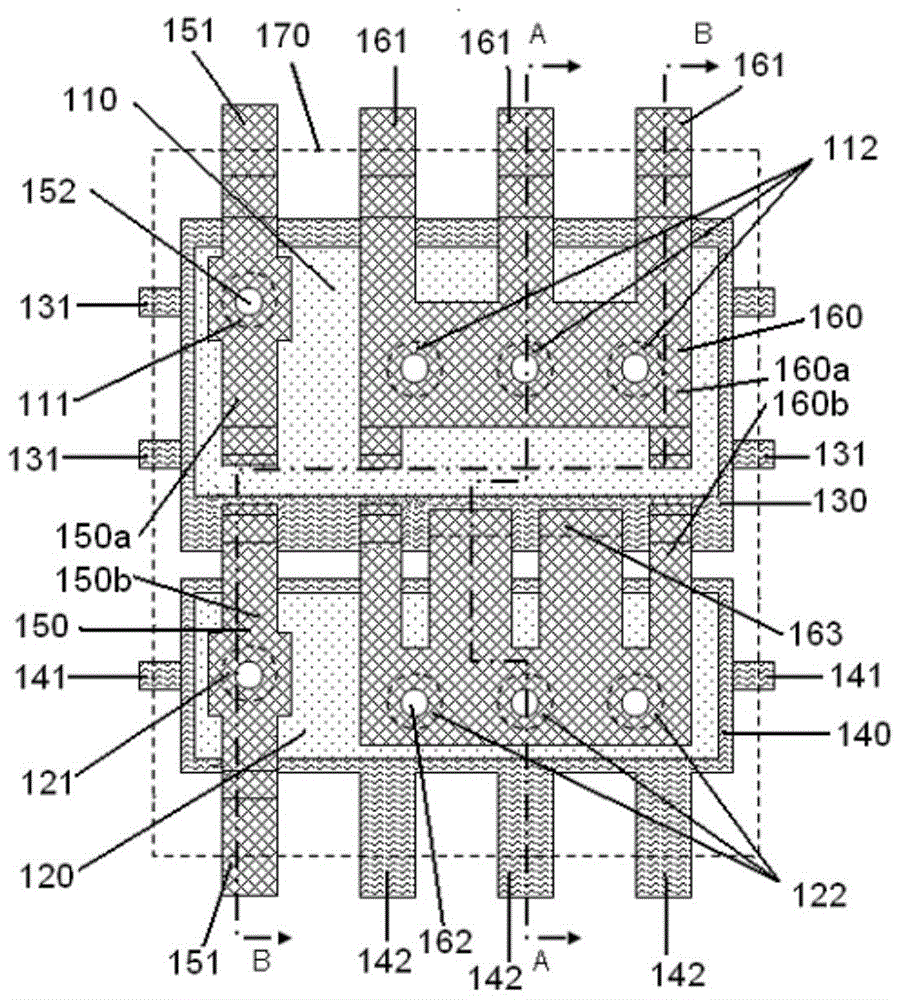
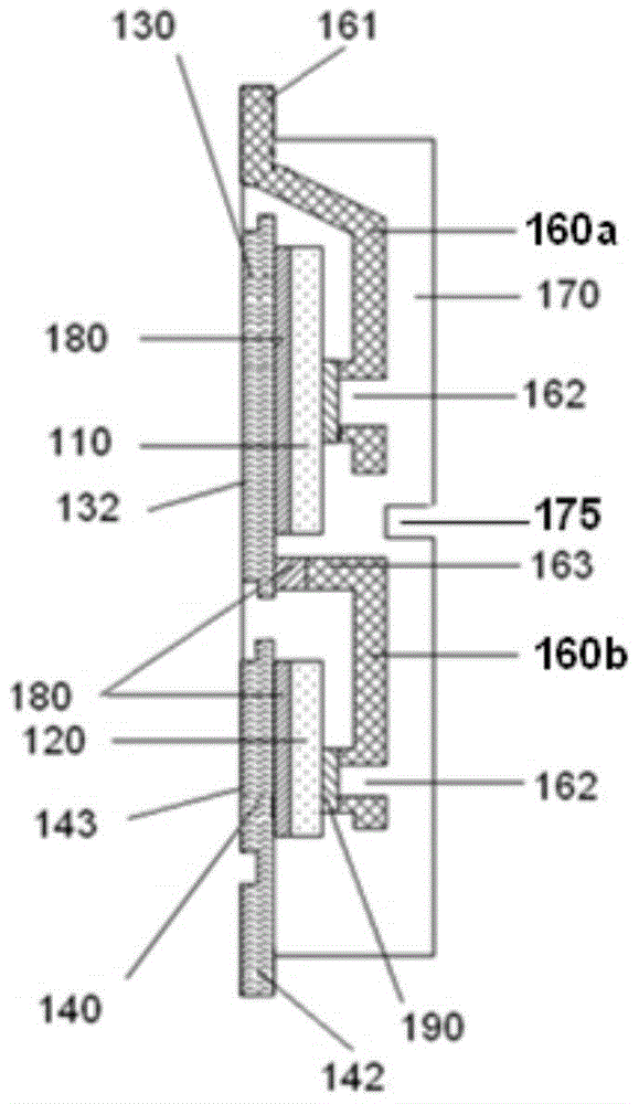
[0088] Embodiment 1. A semiconductor package that is connected by a connecting piece, taking a low-side MOSFET device and a high-side MOSFET co-packaged device as an example, as Figure 2A , Figure 2B and Figure 2CAs shown, it includes first and second two chips, a substrate frame, a plurality of connecting pieces and a plastic package 170 for packaging all the above components; the two chips are respectively the first chip low-side metal-oxide-semiconductor field-effect transistor ( LS MOSFET) 110 and the second chip high-side metal oxide semiconductor field effect transistor (HS MOSFET) 120, the top contact regions of LS MOSFET 110 are gate contact region 111 and source contact region 112 respectively, and the bottom contact region is drain contact region (not shown in the figure), the top contact regions of the HS MOSFET 120 are the gate contact region 121 and the source contact region 122 respectively, and the bottom contact region thereof is the drain contact region (n...

Embodiment 2

[0092] Embodiment 2. A semiconductor package that is connected by a connecting piece, taking a low-side MOSFET device and a high-side MOSFET co-packaged device as an example, as Figure 8A , Figure 8B and Figure 8C As shown, it includes two chips, a substrate frame, a plurality of connecting sheets and a plastic package 270 for encapsulating all the above components; the two chips are the first chip low-side metal-oxide-semiconductor field-effect transistor (LS MOSFET) 210 and The top contact regions of the second chip high-side metal oxide semiconductor field effect transistor (HS MOSFET) 220 and LS MOSFET 210 are gate contact region 211 and source contact region 212 respectively, and their bottom contact regions are drain contact regions (not shown in the figure ), the top contact regions of the HS MOSFET 220 are the gate contact region 221 and the source contact region 222 respectively, and the bottom contact region is the drain contact region (not shown in the figure); ...

Embodiment 3

[0094] Embodiment 3. A semiconductor package that is connected by a connecting piece, taking a low-side MOSFET device and a high-side MOSFET co-packaged device as an example, as Figure 13A , Figure 13B and Figure 13CAs shown, it includes two chips, a substrate frame, a connecting sheet and a plastic package 370 for encapsulating all the above components; the two chips are respectively a low-side metal oxide semiconductor field effect transistor (LS MOSFET) 310 and a high-side metal oxide HS MOSFET 320, the top contact regions of LS MOSFET 310 are gate contact region 311 and source contact region 312 respectively, and the bottom contact region is drain contact region (not shown in the figure), the top contact region of HS MOSFET 320 The contact regions are gate contact region 321 and source contact region 322 respectively, and the bottom contact region is a drain contact region (not shown in the figure); a substrate frame, which includes a substrate frame first chip holder ...


PUM


Abstract

The invention discloses a semiconductor package for internal connection with connecting sheets, comprising: a plurality of chips, each of which has a plurality of top contact areas and bottom contact areas; a plurality of substrates for placing the The chip, the bottom contact area of ​​the chip is electrically connected to the substrate, and the substrate is provided with a plurality of external pins of the substrate; the connecting piece, the connecting piece is connected to a plurality of chips, and is used to connect a plurality of chips correspondingly arranged a plurality of top contact areas, thereby fixing the plurality of chips, and the ends of the connecting sheets are connected to the outside as the pins of the chips; a plastic package is used for packaging chips, substrates, and connecting sheets. The present invention In the process of manufacturing, multiple chips are fixedly connected through one or more connecting pieces, then packaged, and finally the connecting pieces are separated by cutting or grinding on the top of the package. Due to the fixed connection function of the connecting pieces, the present invention avoids the need for chips to be processed in the process. Misalignment during the process affects the circuit performance of the chip.

Description

technical field [0001] The invention relates to a semiconductor packaging structure and a manufacturing method, in particular to a semiconductor packaging and a manufacturing method thereof which are connected by connecting sheets. Background technique [0002] In order to meet the needs of miniaturization of electronic products, multi-chip semiconductor packaging has become a trend, and the semiconductor packaging of multi-chip modules carries multiple chips in a single package. [0003] For example, in the Chinese patent authorization announcement number CN201063342Y, a multi-chip packaging structure is disclosed, including: a first lead frame, including a first chip seat, a first inner pin and a second outer pin; a second lead frame, including a first Two chip seats and second inner pins; the second lead frame is located above or below the first lead frame, and the first lead frame is electrically connected to the second lead frame through the connector; the first chip is...

Claims


Application Information

Patent Timeline
Patent Type & Authority Patents(China)
IPC IPC(8): H01L21/50H01L21/60H01L21/56
CPCH01L2224/48091H01L2224/73265H01L2924/13091
Inventor 鲁军刘凯薛彦迅
Owner ALPHA & OMEGA SEMICON INT LP
Why Eureka
Try Eureka