
Online measuring method used during optical fiber alignment base array manufacturing with silicon substrate technology

An optical fiber alignment and pedestal technology, which is applied in the photoengraving process, optics, measuring device and other directions of the pattern surface, can solve the problems of measurement value error and the accuracy cannot meet the requirements of mass production, etc., and achieve high-precision online line width monitoring. Effect

Active Publication Date: 2014-06-11
SHANGHAI HUAHONG GRACE SEMICON MFG CORP
View PDF5 Cites 2 Cited by
  • Summary
  • Abstract
  • Description
  • Claims
  • Application Information

AI Technical Summary

Problems solved by technology

However, the size of the optical fiber process is on the order of hundreds of microns. Since the size of the display screen of the equipment is certain, the size of the optical fiber is on the order of hundreds of microns, which is thousands of times that of the semiconductor integration process, so the measurement magnification is one thousandth of that of the semiconductor process. The error of the measured value is very large, and the accuracy cannot meet the requirements of mass production.

Method used


Image

  • Online measuring method used during optical fiber alignment base array manufacturing with silicon substrate technology
  • Online measuring method used during optical fiber alignment base array manufacturing with silicon substrate technology
  • Online measuring method used during optical fiber alignment base array manufacturing with silicon substrate technology

Examples


Embodiment Construction

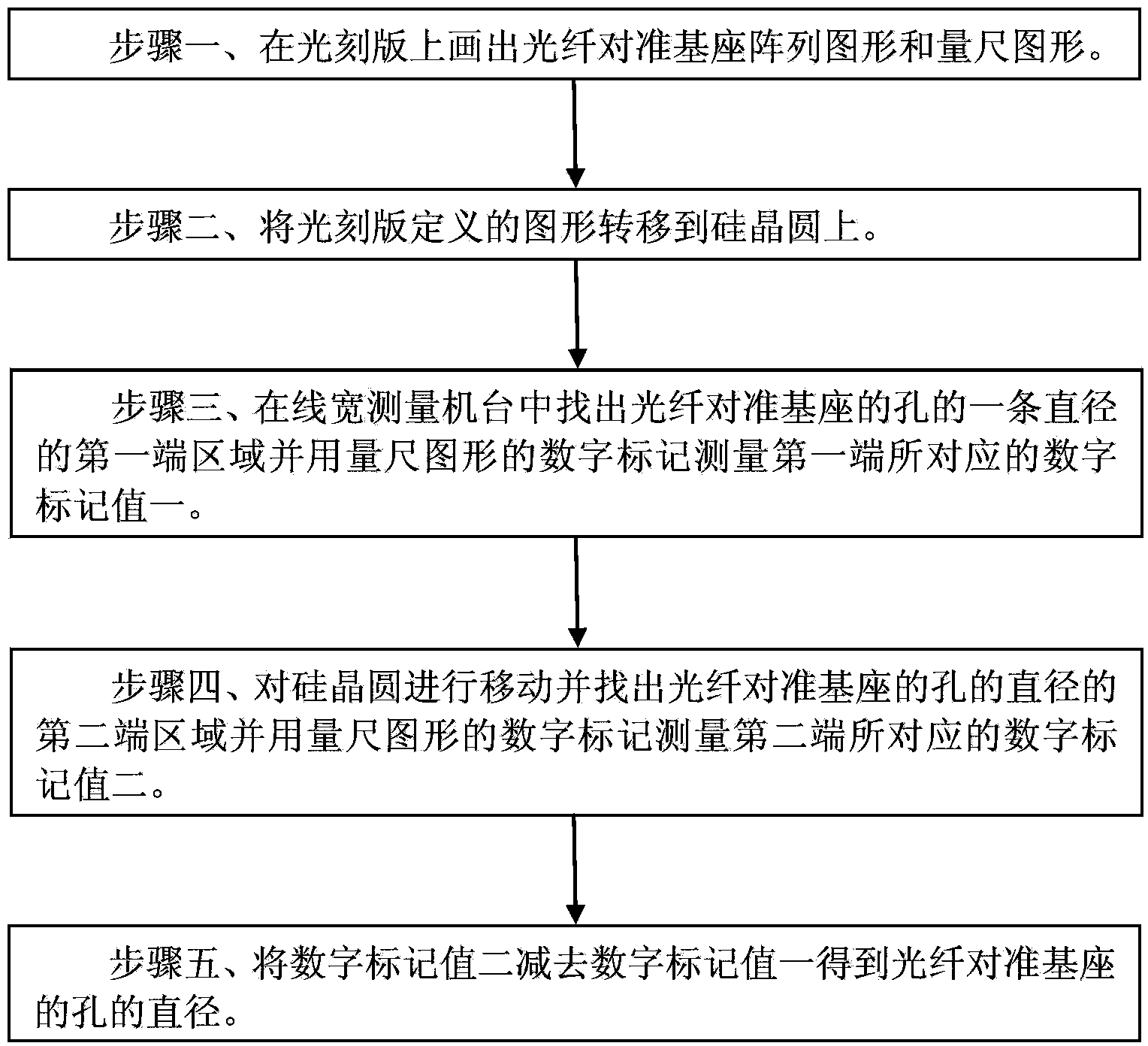
[0021] like figure 1 As shown, it is a flow chart of the method of the embodiment of the present invention; the online measurement method for making an optical fiber alignment base array in the silicon-based process of the embodiment of the present invention includes the following steps:

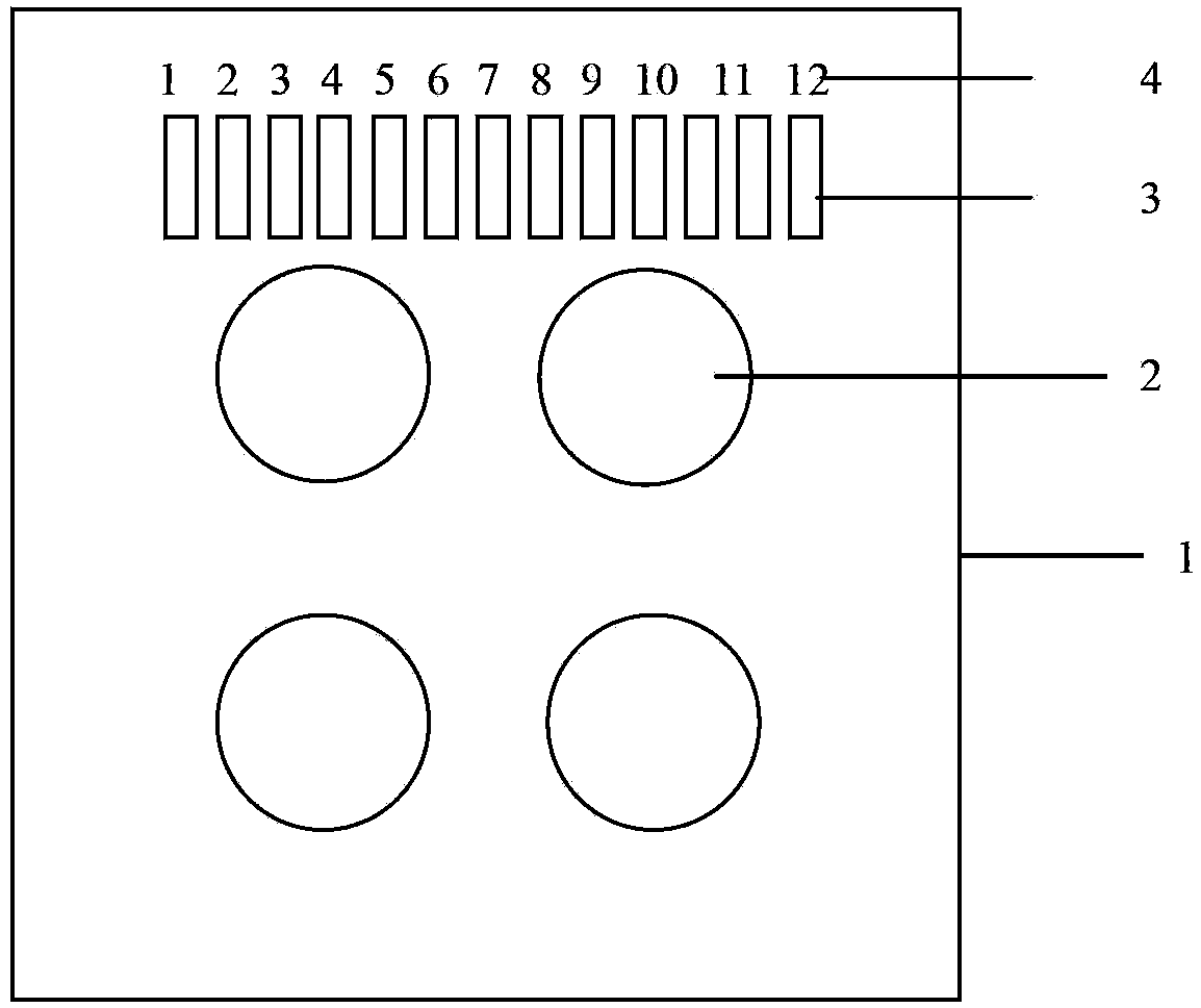
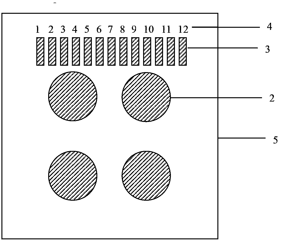
[0022] Step one, as figure 2 As shown, the photoresist plate 1 is made, and the optical fiber alignment base array pattern and the scale figure 3 are drawn on the photoresist plate 1, and the fiber alignment base array pattern defines the holes of the fiber alignment base 2 arrays of size and permutation.

[0023] The scale figure 3 is composed of a series of bar figures with fixed line width and spacing, the line width of the bar figures is 0.1 micron to 1 micron, and the distance between two adjacent bar figures is 0.1 Micron~1 micron, the sum of the line size and spacing of each of the bar graphics of the scale figure 3 is fixed, and the sum of the line size and spacing of each of the ...


PUM

PropertyMeasurementUnit
Diameteraaaaaaaaaa

Abstract

The invention discloses an online measuring method used during optical fiber alignment base array manufacturing with the silicon substrate technology. The method comprises the steps of manufacturing a photolithography mask, manufacturing a measuring scale graph beside a hole of the graph of an optical fiber alignment base array, setting the line width of each line of the measuring scale graph to be smaller than the size of the hole of the graph of the optical fiber alignment base array by two orders of magnitudes, and making the line width and intervals of the lines of the measuring scale graph unchanged; transferring the graph of the photolithography mask to a silicon wafer; measuring a first numerical flag value corresponding to the first end of the hole of the optical fiber alignment base with numerical flags of the measuring scale graph in a line width measuring machine table; measuring a second numerical flag value corresponding to the second end of the hole of the optical fiber alignment base with numerical flags of the measuring scale graph in the line width measuring machine table; obtaining the diameter of the hole of the optical fiber alignment base based on the difference between the first numerical flag value and the second numerical flag value. According to the method, the measurement accuracy of the size of the optical fiber alignment base array can be improved by two orders of magnitudes, and high-accuracy online line width measurement of large products can be achieved.

Description

technical field [0001] The invention relates to a semiconductor integrated circuit manufacturing process method, in particular to an online measurement method for fabricating an optical fiber alignment base array in a silicon-based process. Background technique [0002] At present, the application of optical communication devices is becoming more and more extensive, and the fiber-to-the-home project has also begun to be gradually implemented in most parts of the country. Multiple optical fiber channels are required for optical signal processing in an optical system, and long and thin optical fibers need to be fixed on a large number of optical fiber alignment bases to ensure that the quality of the fixed optical fibers meets system requirements. Therefore, the optical fiber alignment base needs to meet the requirements of high alignment accuracy and stable process in order to meet the optical signal efficiency without too much loss. At present, the fiber through-hole base m...

Claims


Application Information

Patent Timeline
IPC IPC(8): G01B21/10G02B6/13G03F7/00
Inventor 陈瑜袁苑罗啸
Owner SHANGHAI HUAHONG GRACE SEMICON MFG CORP
Learn More