

Microscopic section rapid digital scanning device and method with real-time focusing function
A technology of microsectioning and digital scanning, applied in the field of microscopy, which can solve the problems of loss of focal plane, large measurement range, poor accuracy, etc.
- Summary
- Abstract
- Description
- Claims
- Application Information
AI Technical Summary
Problems solved by technology
Method used
Image

Examples
Embodiment 1
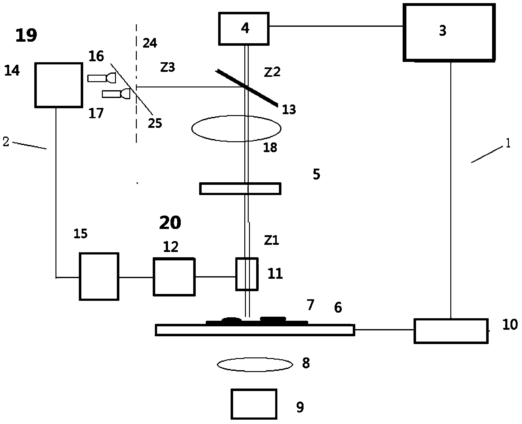
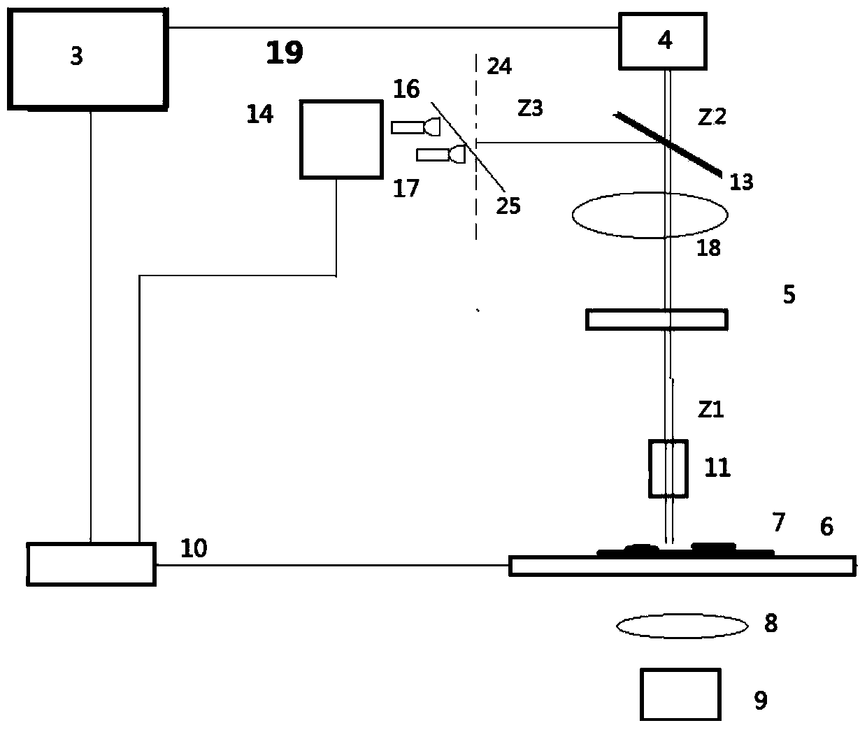
[0064] Combined with accompanying drawings 1 (A), 1 (B), 2 (A), 2 (B).
[0065] A fast digital scanning device for microsections with real-time focusing of the present invention is a scanning device for quickly acquiring all or a considerable part of digital images of microsections, comprising: a digital microscopic imaging system 1 and a The real-time focusing device 2 matched with it. The digital microscopic imaging system 1 includes at least a computer 3, an image detection device 4 connected to the computer to realize photoelectric conversion, and a microscopic optical imaging system 5 between the sample 7 placed on the automatic stage 6 and the image detection device 4 . The microscopic optical imaging system 5 includes at least one objective lens 11 and a matched tube lens 18 , and a filter cube may be placed between the objective lens and the tube lens. The digital micro-imaging system 1 also includes at least an illumination optical system 8 and an illumination light...
Embodiment 2
[0078] Combined with accompanying drawings 1 (A), 1 (B), 3 (A), 3 (B).
[0079] Compared with the first embodiment, this embodiment only expands the detection range of the defocus amount of the first embodiment. Therefore, except that a few more optical signal detection elements are placed, the rest of the components are the same, and will not be repeated here, and only the special part of this embodiment, that is, the defocus measurement part, will be described below.
[0080] When the defocus distance 2d that can be effectively measured by a pair of optical signal detection elements along the first straight line cannot meet the requirements, multiple pairs of optical signal detection elements can be placed along the first straight line. Figure 3(A) shows the situation where two pairs of four optical signal detection elements are placed. They are projected on the XY plane along the X direction, and the defocus range of the focal plane that can be measured by the first pair of...
Embodiment 3
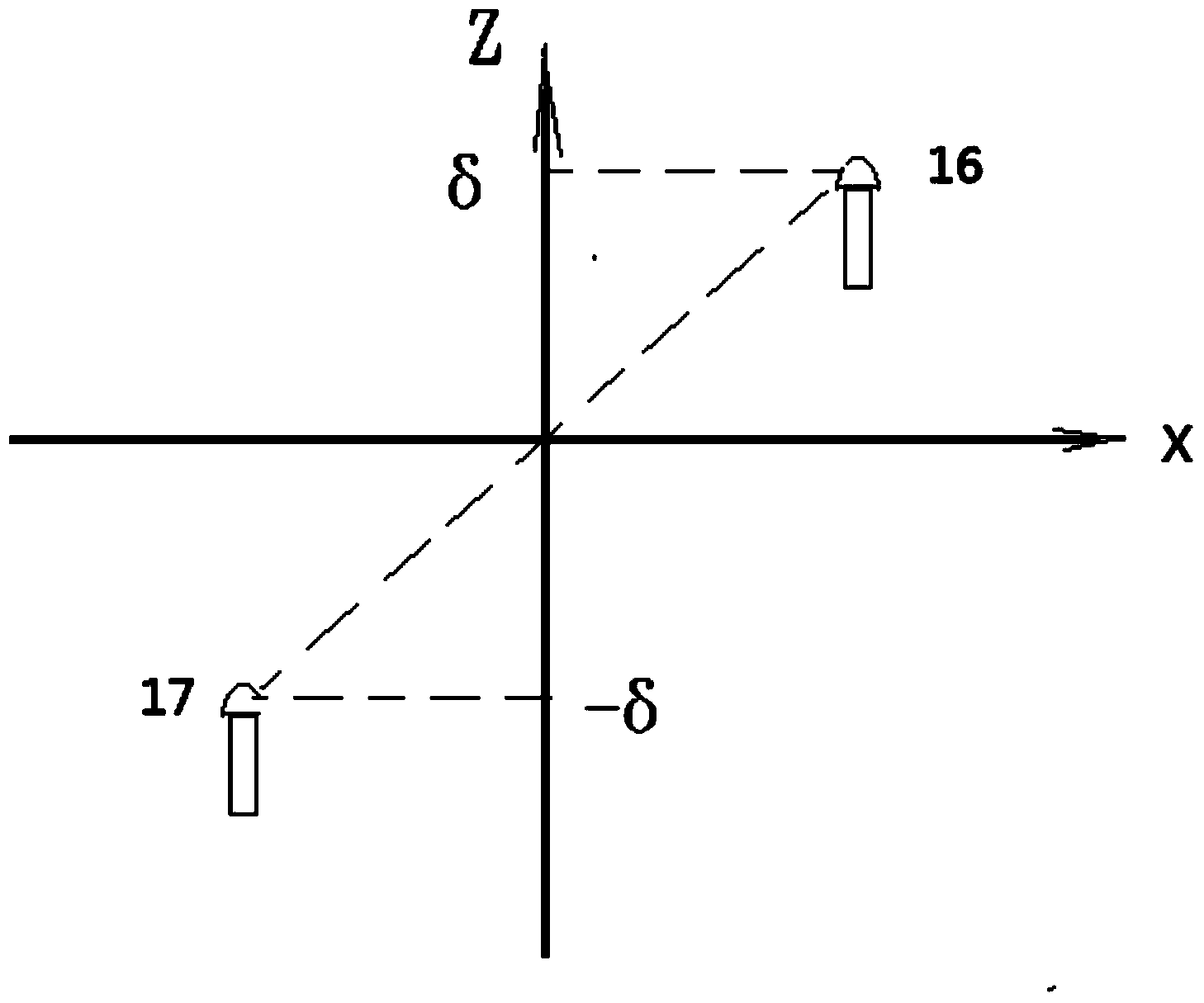
[0087] Compared with the first embodiment, this embodiment is that a pair of optical signal detection elements are placed in the first linear direction, and their projection on the XY plane is along the X direction, and they form an angle α with the XY plane. On this basis, a second pair of optical signal detection elements is placed in the second linear direction, and the angle between them and the XY plane is also α, and the projection of the second pair on the XY plane is parallel to the Y direction. Therefore, compared with Embodiment 1, except that a pair of optical signal detection elements are placed in the Y direction, other components are the same, and will not be described again here.
[0088] In this implementation example, the defocus measurement ranges of the photoelectric conversion in the X / Y direction projected on the XY plane are between [-d, d]. When the defocus measurement device along the X direction measures the defocus amount as x, and the defocus measure...
PUM
 Abstract
Description
Claims
Application Information