Low-power-consumption chip level atomic clock physical packaging device

A chip-level atomic clock and packaging device technology, applied in the direction of automatic power control, electrical components, etc., can solve problems such as power consumption, and achieve the effects of reducing power consumption, easy implementation, and simple processing

Inactive Publication Date: 2014-06-11
SUZHOU UNIV
View PDF6 Cites 10 Cited by
  • Summary
  • Abstract
  • Description
  • Claims
  • Application Information

AI Technical Summary

Problems solved by technology

[0005] In previous inventions or in the physical packaging of chip-scale atomic clock systems currently in use, this magnetic field is generated by a coil passing a certain current (such as figure 1 shown), which requires power consumption

Method used


Image

  • Low-power-consumption chip level atomic clock physical packaging device
  • Low-power-consumption chip level atomic clock physical packaging device
  • Low-power-consumption chip level atomic clock physical packaging device

Examples


Embodiment 1

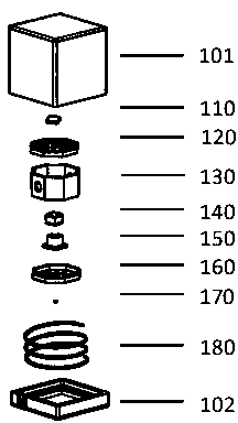
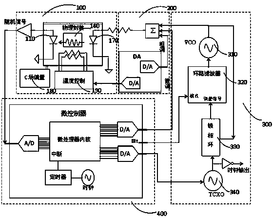
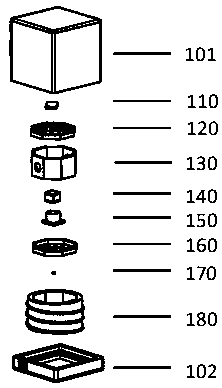
[0026] Embodiment one: see figure 2 As shown, it is a block diagram of an overall system of a chip-level atomic clock, which mainly includes two main parts of a physical package 100 and an electronic circuit. where the physical package 100 can be found in figure 2 As shown, it mainly includes ceramic package 101, photodetector 110, upper bracket 120, frame spacer 130, basic atomic bubble gas chamber 140, CPT resonant cavity 150, 1 / 4 wave plate, lower bracket 160, laser 170, C Field bias module 180 , heating device (ITO thin film) 190 , and base 102 . The alkali metal may be rubidium, cesium or other alkali metals with hyperfine energy level splitting. The C-field bias module 180 can be produced by a coil, a permanent magnet, or a coil and a permanent magnet, see image 3 shown. The C-field bias module 180 in the present invention can be produced by a permanent magnet or by cooperation of a permanent magnet and a coil. This greatly reduces the current through the coil, t...

Embodiment 2

[0030] Embodiment two: see Figure 4 As shown, permanent magnet poles 181 with different properties can be placed at both ends of the physical package 100 , and the permanent magnets 181 generate a magnetic field along the axial direction of the physical package 100 . The magnetic field can be used to separate each Zeeman magneton energy level, so that the 0-0 magneton energy level transition of the ground state can be used as the transition line of the atomic clock. The magnetic poles 181 shown can be in various shapes such as circular, square, polygonal, and the like. The magnetic poles 181 are placed on both sides of the upper and lower supports 120, 160 of the physical package. If the requirement for the accuracy of the magnetic field is relatively high, we can simultaneously surround the coil 40 outside the frame spacer 130 of the physical package 100 to fine-tune the magnetic field strength.

Embodiment 3

[0031] Embodiment three: see Figure 5 and 6 As shown, the permanent magnet can also be cylindrical 182 or square cylindrical 183 . Cylindrical 182 or square cylindrical 183 permanent magnets can generate a magnetic field along the axial direction of the physical package 100, and the physical package 100 is placed in the cylindrical 182 or square cylindrical 183 permanent magnets. The magnetic field produced by the permanent magnets can realize atomic The individual Zeeman magneton energy levels of hyperfine energy level splitting are separated, thereby satisfying the conditions for the normal operation of the physical package 100 .


PUM


Abstract

The invention discloses a low-power-consumption chip level atomic clock physical packaging device which comprises an external package, an upper support, a lower support, a frame space device and an internal element. The external package is composed of a ceramic package body and a base. The internal element comprises a laser, a photoelectric detector, an alkaline atom bubble air chamber, a 1/4 wave plate and a C-field bias module. The C-field bias module comprises a permanent magnet assembly which generates a magnetic field in the physical packaging axial direction. The magnetic field generated by a permanent magnet can totally or partially replace a magnetic field generated by a coil in original chip level atomic clock physical packaging, currents flowing through the coil can be minimum, and therefore energy consumption of chip level atomic clock packaging can be greatly reduced.

Description

technical field [0001] The invention relates to a physical packaging device for an atomic clock, in particular to a physical packaging device for a chip-level atomic clock with low power consumption. Background technique [0002] As one of the seven most basic physical quantities, time (frequency) has the highest reproduction accuracy. Since the world's first atomic clock was successfully developed in 1949, the accuracy of time units has developed rapidly, increasing by an order of magnitude every 10 years. In addition to providing time and frequency output, atomic clocks are also widely used in navigation and positioning, communications, missile and satellite positioning, astronomical observation, geodetic surveying, calibration of precision instruments, power grid regulation, and high-speed traffic management, and in the past 50 years Has become one of the indispensable devices. [0003] With the rapid development of electronic technology and control technology, the rese...

Claims


Application Information

Patent Timeline
Patent Type & Authority Applications(China)
IPC IPC(8): H03L7/26
Inventor 韩胜男乔东海汤亮张忠山季磊栗新伟
Owner SUZHOU UNIV
Why Eureka
Try Eureka