

Organic electroluminescent device and display device
An electroluminescent device and luminescent technology, applied in the direction of organic semiconductor devices, electric solid devices, electrical components, etc., can solve the problem of reducing the internal quantum efficiency of organic electroluminescent devices, reducing the external quantum efficiency of organic electroluminescent devices, strong Hole blocking effect and other issues can be achieved to improve the display effect, improve the external quantum efficiency, and increase the excitation rate.
- Summary
- Abstract
- Description
- Claims
- Application Information
AI Technical Summary
Problems solved by technology
Method used
Image

Examples
Embodiment 1
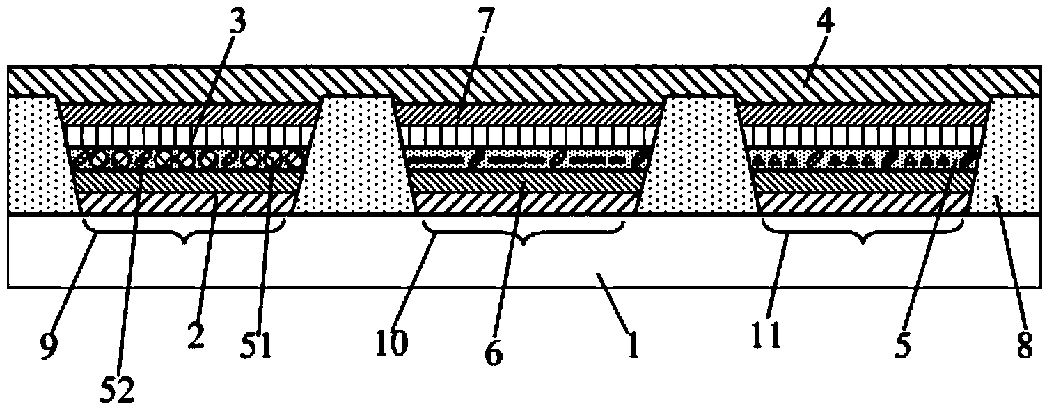
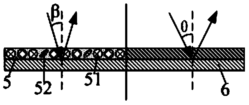
[0028] This embodiment provides an organic electroluminescent device, such as figure 1 As shown, it includes a substrate 1, and an opaque electrode 2, a light-emitting layer 3, and a light-transmitting electrode 4 arranged above the substrate 1. The light-emitting layer 3 is arranged between the opaque electrode 2 and the light-transmitting electrode 4. 3 and the opaque electrode 2 are also provided with a scattering layer 5, which can totally reflect the light emitted by the light-emitting layer 3 towards the side of the scattering layer 5.
[0029] It should be noted that organic electroluminescent devices are classified into top-emission organic electroluminescent devices and bottom-emission organic electroluminescent devices according to the direction in which light is emitted. The top emission type means that the top surface of the organic electroluminescent device is a light-transmitting surface, and light is emitted from the top surface of the organic electroluminescent...
Embodiment 2
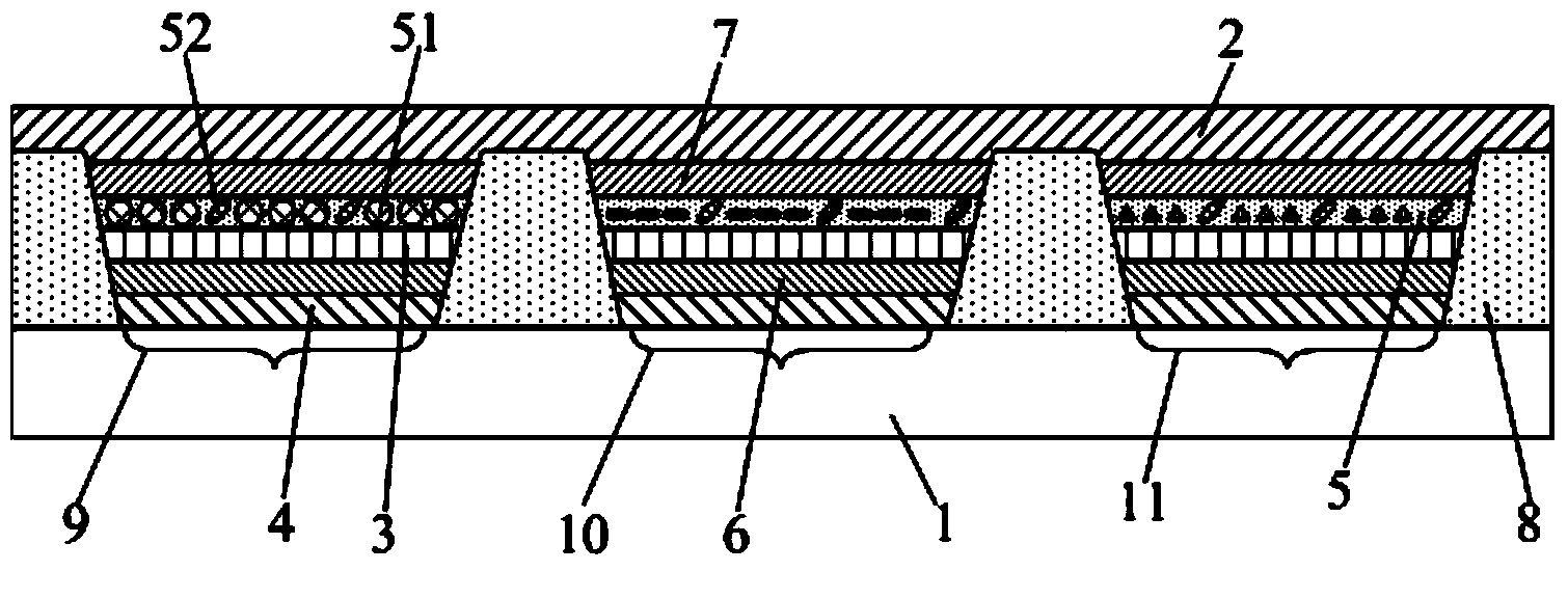
[0044] This embodiment provides an organic electroluminescent device, which is different from Embodiment 1, such as image 3 As shown, the opaque electrode 2 is a cathode, and the transparent electrode 4 is an anode; correspondingly, the scattering layer 5 is disposed between the cathode and the light-emitting layer 3 ; and the electron transport layer 7 is disposed between the cathode and the scattering layer 5 .
[0045] Compared with the organic electroluminescent device in embodiment 1, in this embodiment, light is emitted from the bottom surface of the organic electroluminescent device, so the organic electroluminescent device provided in this embodiment is a bottom emission type.
[0046] Other structures of the organic electroluminescent device in this embodiment are the same as those in Embodiment 1, and will not be repeated here.
Embodiment 3
[0048] This embodiment provides an organic electroluminescent device, which is different from Embodiment 1, such as Figure 4 As shown, the hole transport layer 6 is disposed between the light emitting layer 3 and the scattering layer 5 .
[0049] Other structures of the organic electroluminescent device in this embodiment are the same as those in Embodiment 1, and will not be repeated here.
PUM
| Property | Measurement | Unit |
|---|---|---|
| Size | aaaaa | aaaaa |
Abstract
Description
Claims
Application Information