Method for preparing magnesium diboride superconductive Josephson junction through secondary mask method

A magnesium diboride and mask technology, which is applied in the field of preparation of superconducting thin film Josephson junctions, can solve the problems of difficult preparation of superconducting Josephson junctions, connectivity, etc., and achieves short annealing time, reduced component diffusion, and temperature rise and fall speed. quick effect

Active Publication Date: 2014-07-02
INST OF ELECTRICAL ENG CHINESE ACAD OF SCI
View PDF2 Cites 5 Cited by
  • Summary
  • Abstract
  • Description
  • Claims
  • Application Information

AI Technical Summary

Problems solved by technology

[0007] From the literature "Si substrate MgB 2 —B—MgB 2 It can be seen from the preparation and characteristics of superconducting SNS Josephson junction" and the preparation method of patent 2011120328538.1 that when they prepare the [Mg / B]-X-[Mg / B] structure precursor film, the bottom magnesium diboride precursor film, Part of the edges of the intermediate barrier layer and the top layer of the magnesium diboride precursor film are aligned, which can easily cause the three layers of films to diffuse and stagger each other at the aligned edges, and connect them into one piece. After annealing, the underlying superconducting film and The phenomenon that the top superconducting thin film is connected, it is difficult to prepare a superconducting Josephson junction

Method used


Image

  • Method for preparing magnesium diboride superconductive Josephson junction through secondary mask method
  • Method for preparing magnesium diboride superconductive Josephson junction through secondary mask method
  • Method for preparing magnesium diboride superconductive Josephson junction through secondary mask method

Examples


Embodiment 1

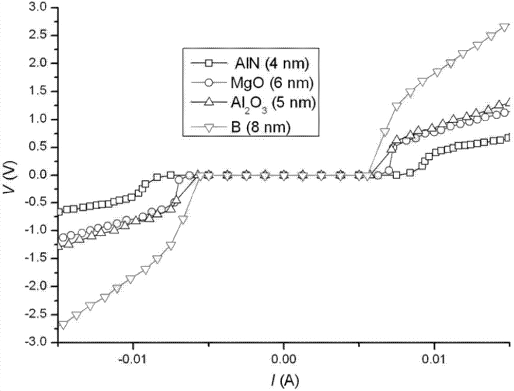
[0052] The preparation of the precursor film in this example was completed in a ZZXS-500 electron beam coating machine, and the electron beam annealing was performed on a self-made EBW-6 electron beam welding machine. The precursor film structure is [Mg(15nm)+B(10nm)] 6 —B(8nm)—[Mg(15nm)+B(10nm)] 5 , the thickness of the precursor film is 283nm, and the size of the substrate SiC is 10.0mm×3.0mm.

[0053] 1. Preparation of precursor film

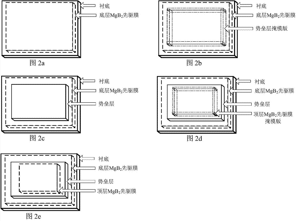
[0054] (1) Preparation of the underlying precursor film

[0055] (1.1) Fix the SiC bare substrate with a size of 10.0mm×3.0mm on the sample workpiece stage;

[0056] (1.2) Place the sample workpiece table in the ZZXS-500 electron beam coating machine and start vacuuming;

[0057] (1.3) Wait for the vacuum degree to be higher than 5×10 -5 After Pa, turn on the quartz crystal thin film coating controller;

[0058] (1.4) Evaporate layer B on the bare SiC substrate, and the number on the display panel of the quartz crystal thin film coating...

Embodiment 2

[0089] The preparation of the precursor film in this example was completed in a ZZXS-500 electron beam coating machine, and the electron beam annealing was performed on a self-made EBW-6 electron beam welding machine. The precursor film is [Mg(12nm)+B(8nm)] 5 —AlN(4nm)—[Mg(12nm)+B(8nm)] 5 , the thickness of the precursor film is 204nm, and the size of the substrate SiC is 10.0mm×3.0mm.

[0090] 1. Preparation of precursor film

[0091] (1) Preparation of the underlying precursor film

[0092] (1.1) Fix the SiC bare substrate with a size of 10.0mm×3.0mm on the sample workpiece stage;

[0093] (1.2) Place the sample workpiece table in the ZZXS-500 electron beam coating machine and start vacuuming;

[0094] (1.3) Wait for the vacuum degree to be higher than 5×10 -5 After Pa, turn on the quartz crystal thin film coating controller;

[0095] (1.4) Evaporate layer B on the bare SiC substrate, and the number on the display panel of the quartz crystal thin film coating controlle...

Embodiment 3

[0126] The preparation of the precursor film in this example was completed in a ZZXS-500 electron beam coating machine, and the electron beam annealing was performed on a self-made EBW-6 electron beam welding machine. The precursor film is [Mg(12nm)+B(8nm)] 5 —Al 2 o 3 (5nm)—[Mg(15nm)+B(10nm)] 3 , the film thickness is 180nm, and the substrate Si size is 10.0mm×3.0mm.

[0127] 1. Preparation of precursor film

[0128](1) Preparation of the underlying precursor film

[0129] (1.1) Fix the bare Si substrate with a size of 10.0mm×3.0mm on the sample workpiece stage;

[0130] (1.2) Place the sample workpiece table in the ZZXS-500 electron beam coating machine and start vacuuming;

[0131] (1.3) Wait for the vacuum degree to be higher than 5×10 -5 After Pa, turn on the quartz crystal thin film coating controller;

[0132] (1.4) Evaporate layer B on the bare Si substrate, and the number on the display panel of the quartz crystal thin film coating controller is After stop c...


PUM

PropertyMeasurementUnit
thicknessaaaaaaaaaa
thicknessaaaaaaaaaa
lengthaaaaaaaaaa

Abstract

Disclosed is a method for preparing a magnesium diboride superconductive Josephson junction through a secondary mask method. According to the method, an electron beam is adopted to carry out annealing on an interlayer type (sandwich type) magnesium diboride Josephson junction precursor film. The interlayer type magnesium diboride Josephson junction precursor film is a (Mg/B)-X-(Mg-B) structure precursor film prepared through the secondary mask method, X represents a standard conductor layer N or an insulation layer I, magnesium elementary substance and boron elementary substance in the precursor film are made to generate a chemical reaction within the annealing time of a second magnitude order, finally the SNS type or SIS type magnesium diboride superconductive Josephson junction of a MgB2-X-MgB2 structure is generated, and S represents a superconductive layer.

Description

technical field [0001] The invention relates to a preparation method of a superconducting thin film Josephson junction. Background technique [0002] The Josephson (Josephson) junction is the key to the application of superconducting weak electricity. Since the discovery of the magnesium diboride superconductor (Nature410(2001) 63) with a critical transition temperature of 39K in January 2001 by Akimitsu et al. in Japan, scientists from various countries have paid attention to Josephson junction. The preparation of Mori junction has aroused great interest, actively exploring various methods to prepare high-quality MgB 2 Superconducting Josephson junction. MgB 2 It has a high critical transition temperature Tc, a simple structure, a grain boundary transparent to the transmission current, weak anisotropy and a long coherence length (ξab(0)=3.7~12nm). Because its critical temperature is much higher than that of conventional superconductors, the coherence length and carrier c...

Claims


Application Information

Patent Timeline
Patent Type & Authority Applications(China)
IPC IPC(8): H01L39/24
Inventor 孔祥东李晓娜韩立初明璋许壮
Owner INST OF ELECTRICAL ENG CHINESE ACAD OF SCI
Why Eureka
Try Eureka