Preparation method of compound thin film for solar battery
A technology for preparing solar cells and thin films, which is applied in the manufacture of circuits, electrical components, and final products. It can solve the problems of unsuitable continuity, high-capacity and low-cost industrial production, photovoltaic cells that are difficult to form a competitive advantage, production technology and cost. and other problems, to achieve the effect of short annealing time, large grain size and short production cycle
- Summary
- Abstract
- Description
- Claims
- Application Information
AI Technical Summary
Problems solved by technology
Method used
Image
Examples
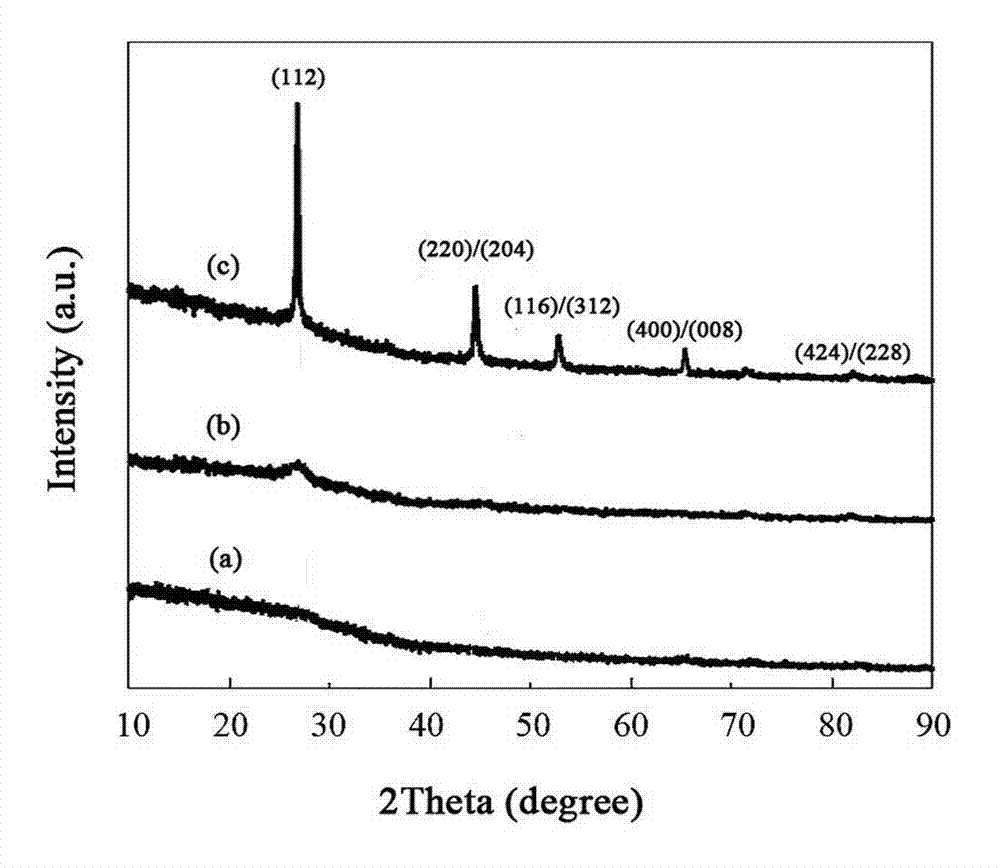
Embodiment 1
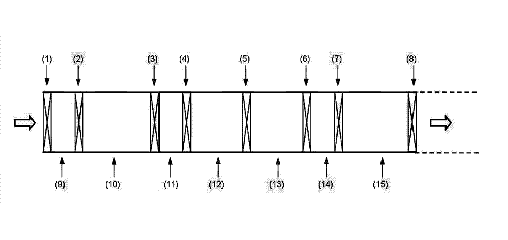
[0021] Fabrication of CuIn with a brass structure phase with a thickness of 1000 nm at a sputtering power of 3 kW 1-x Ga x Se 2-y S y film. Such as figure 1 Shown, the present invention is preparing CuIn 1-x Ga x Se 2-y S y For the thin film, a continuous multi-chamber equipment and automatic control system are used to realize the deposition preparation, rapid heat treatment, cooling and passivation annealing of the thin film in a closed state. The specific steps are as follows:
[0022] 1. Put the cleaned and dried glass substrate or the Mo-coated glass substrate on the substrate holder, and pass the equilibrium gas Ar into the transition chamber 9 to an atmospheric pressure of 1.0×10 5 Pa, open the gate valve 1, the substrate holder enters the transition chamber 9 under the action of the transmission system, close the gate valve 1, pump the transition chamber 9 to 1.0×10 -5 After Pa, the balance gas Ar is introduced to 0.8Pa,
[0023] 2. Open the gate valve 2, wai...
Embodiment 2
[0031] Preparation of CuIn with chalcopyrite structure phase with a thickness of 1500 nm at a sputtering power of 6 kW 1-x Ga x Se 2-y S y film.
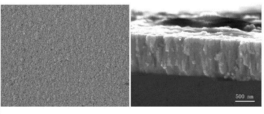
[0032] Using the same steps as in Example 1, the advancing speed of the substrate in the deposition chamber was 15 mm / min, and a little H was introduced during sputtering. 2 S. Different sputtering power on CuIn 1-x Ga x Se 2-y S y The microstructure of the film has a significant impact, and the surface morphology and crystallographic properties also change accordingly, such as Figure 4 shown.
Embodiment 3
[0034] Preparation of CuIn with chalcopyrite structure phase with a thickness of 1000 nm at a sputtering power of 6 kW 1-x Ga x Se 2-y S y film.
[0035] Using the same steps as in Example 1, the advancing speed of the substrate in the deposition chamber was 20 mm / min, and a little H was introduced during sputtering. 2 S. CuIn 1-x Ga x Se 2-y S y The thickness of the film has a significant effect, as Figure 5 shown.
PUM
 Abstract
Description
Claims
Application Information


