Image sensor and method of forming same

An image sensor and doped region technology, which is applied in the direction of electric solid-state devices, semiconductor devices, electrical components, etc., can solve the problems of poor image sensor performance, achieve good performance, and improve the effect of full well capacitance

Inactive Publication Date: 2019-11-01
HUAIAN IMAGING DEVICE MFGR CORP
View PDF4 Cites 2 Cited by
  • Summary
  • Abstract
  • Description
  • Claims
  • Application Information

AI Technical Summary

Problems solved by technology

[0004] However, as the size of the pixel unit continues to shrink, the full-well capacitance of the photodiode also decreases, resulting in poor performance of the image sensor

Method used


Image

  • Image sensor and method of forming same
  • Image sensor and method of forming same
  • Image sensor and method of forming same

Examples


Embodiment Construction

[0021] As mentioned in the background, the performance of image sensors formed by existing methods is relatively poor.

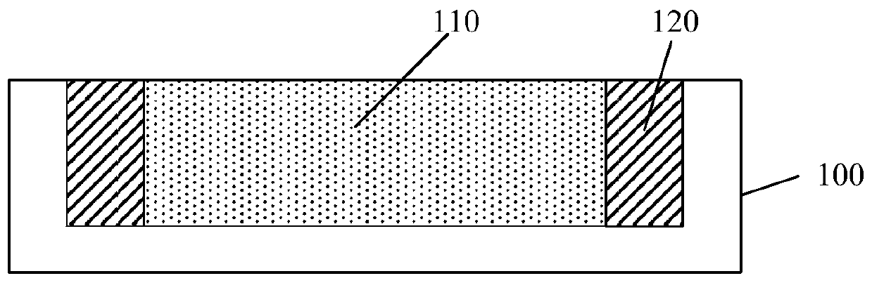
[0022] figure 1 It is a schematic diagram of the cross-sectional structure of an image sensor.

[0023] Please refer to figure 1 , the image sensor includes: a semiconductor substrate 100; a photoelectric doped region 110 located in the semiconductor substrate 100, and the conductivity type of the photoelectric doped region 100 is opposite to that of the semiconductor substrate 100; The isolation region 120 on the sidewall of the impurity region 110 , and the conductivity type of the isolation region 120 is opposite to that of the photoelectric doped region 110 .

[0024] In the above structure, generally there is a well region (not shown in the figure) in the semiconductor substrate 100, and there are first dopant ions in the well region; there are second dopant ions in the photoelectric doped region 110 , the conductivity types of the first dopant ions ...


PUM


Abstract

The present invention provides an image sensor and a method of forming the same. The method comprises the steps of: providing a semiconductor substrate; forming an initial photo-doped region in the semiconductor substrate; forming mutually separated initial isolation regions in the initial photo-doped region, the initial isolation regions being doped with first ions and second ions, the conductivity type of the first ions being opposite to the conductivity type of the initial photo-doped region, the conductivity type of the second ions being the same as the conductivity type of the initial photo-doped region, and the diffusion rate of the second ions being larger than that of the first ions; performing heat treatment to diffuse the first ions and the second ions in the initial isolation region, and forming a main photo-doped region, mutually separated isolation regions and mutually separated additional photo-doped regions in the initial photo-doped region, wherein the conductivity typeof the additional photo-doped regions is the same as that of the main photo-doped region, and the conductivity type of the isolation regions is opposite to that of the main photo-doped region. The image sensor formed by adopting the method is good in performance.

Description

technical field [0001] The invention relates to the field of semiconductor manufacturing, in particular to an image sensor and a forming method thereof. Background technique [0002] With the continuous improvement of semiconductor technology, the image sensor (Image Sensor), as a basic device for information acquisition, has been more and more widely used in modern society. Complementary Metal Oxide Semiconductor (CMOS) image sensor is a fast-growing solid-state image sensor. Since the image sensor part and the control circuit part of the CMOS image sensor are integrated in the same chip, the volume of the CMOS image sensor Compared with the traditional charge-coupled device (CCD) image sensor, it has advantages of small size, low power consumption, and low price, and is also easier to popularize. [0003] Existing CMOS image sensors include photosensors for converting optical signals into electrical signals. The photosensors are photodiodes formed in a silicon substrate, ...

Claims


Application Information

Patent Timeline
Patent Type & Authority Applications(China)
IPC IPC(8): H01L27/146
CPCH01L27/1463H01L27/14643H01L27/14683H01L27/14698
Inventor 阿久津良宏
Owner HUAIAN IMAGING DEVICE MFGR CORP
Why Eureka
Try Eureka