Infrared imaging spectrometer based on light beam splitter and manufacturing method
A technology of infrared imaging spectrometer and beam splitter, which is applied in the fields of optics, instruments, spectrum investigation, etc. It can solve the problems of large volume and poor real-time performance of beam splitting devices, and achieve the effects of large luminous flux, stable structure, and high signal-to-noise ratio
- Summary
- Abstract
- Description
- Claims
- Application Information
AI Technical Summary
Problems solved by technology
Method used
Image

Examples
specific Embodiment approach 1
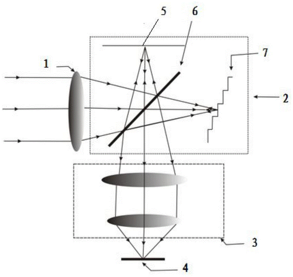
[0029] Specific implementation mode 1. Combination Figure 1 to Figure 2 To illustrate this embodiment, the infrared imaging spectrometer based on a lightweight beam splitter is composed of a front imaging system 1, an interference system 2, a rear imaging beam reduction system 3 and an infrared CCD 4, and the interference system 2 includes a grid type beam splitter 6. Multi-level stepped micro-mirror 7 and plane mirror 5; at a certain moment, the light emitted by the ground target object is imaged by the front-end imaging system and then divided into two beams of coherent light with the same intensity by the grid-type beam splitter 6. The beam of light is reflected by the beam splitter and is imaged on the plane mirror 5 , and the other beam of light is transmitted by the grid beam splitter 6 and then imaged on the multi-level stepped micro-mirror 7 . Wherein the different reflective surfaces of the multi-level stepped micro-mirror 7 correspond to images formed in a certain fie...
specific Embodiment approach 2
[0036] Specific embodiment two, combine Figure 4 to Figure 6 Describe this embodiment, this embodiment is the manufacturing method of the infrared imaging spectrometer based on the light beam splitter described in the specific embodiment 1, this method is realized by the following steps:
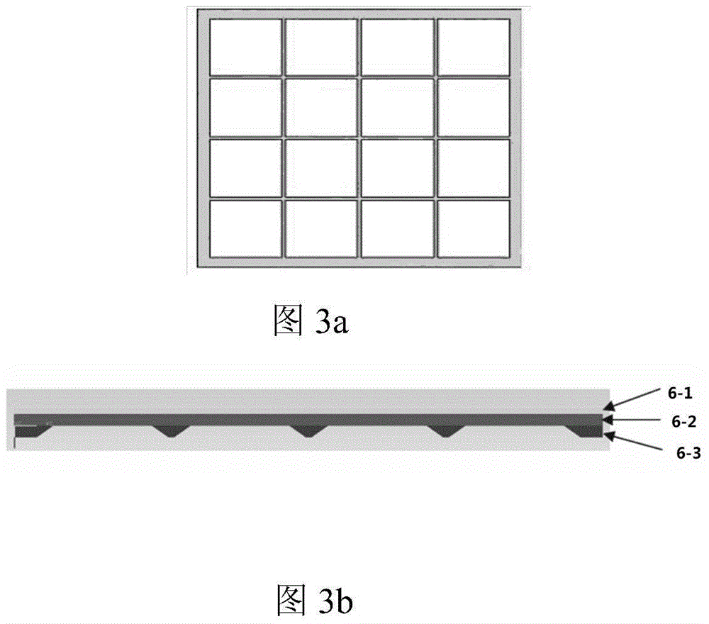
[0037] a. To make the substrate of the imaging spectrometer, select aluminum, copper, titanium, stainless steel or silicon as the substrate material, use the substrate material to make the substrate of the system according to the designed size requirements, and polish the upper surface; the roughness of the polished surface is less than or equal to 10 Micron, the flatness is less than or equal to 50 microns.
[0038] b. Make reference lines perpendicular to each other on the polished substrate by precision machining or photolithography and etching based on MOEMS technology as reference lines for the first optical axis and the second optical axis. According to the analysis and calculation, ...
PUM
| Property | Measurement | Unit |
|---|---|---|
| Flatness | aaaaa | aaaaa |
| Height | aaaaa | aaaaa |
Abstract
Description
Claims
Application Information
 - Generate Ideas
- Intellectual Property
- Life Sciences
- Materials
- Tech Scout
- Unparalleled Data Quality
- Higher Quality Content
- 60% Fewer Hallucinations
Browse by: Latest US Patents, China's latest patents, Technical Efficacy Thesaurus, Application Domain, Technology Topic, Popular Technical Reports.
© 2025 PatSnap. All rights reserved.Legal|Privacy policy|Modern Slavery Act Transparency Statement|Sitemap|About US| Contact US: help@patsnap.com